Substrate with built-in passive element

a passive element and substrate technology, applied in the direction of inductance, printed circuit non-printed electric components association, semiconductor/solid-state device details, etc., can solve the problems of affecting the advantage of tsv technology, affecting the performance of tsv, and increasing the wiring inductan

Active Publication Date: 2014-07-24
NAPRA
View PDF10 Cites 15 Cited by
  • Summary
  • Abstract
  • Description
  • Claims
  • Application Information

AI Technical Summary

Benefits of technology

[0010]It is an object of the present invention to provide a thin substrate in which built-in passive elements are arranged at high density.

Problems solved by technology

However, when the operation is made faster by using the TSV (through silicon via) technology, for example, switching noise generated in a semiconductor chip may cause a malfunction of the integrated circuit.
However, if a capacitor is mounted on the circuit board as an additional component, the wiring inductance increases because of a large connection distance between the capacitor and the semiconductor chip, impairing the advantage of the TSV technology.
In Japanese Unexamined Patent Application Publication No. 2007-220943, however, since the first thin-film multilayer wiring layer, the thick-film pattern electrode, the thick-film passive element film, the second thin-film multilayer wiring layer and the thin-film passive element film are formed on the silicon substrate, the entire thickness of the wiring circuit board having passive elements built therein inevitably becomes large.
Moreover, since the planar passive elements are arranged on the substrate, it is difficult to arrange the passive elements at high density.
Therefore, it is less suitable for the TSV technology intended for high-density packaging.

Method used


Image

  • Substrate with built-in passive element
  • Substrate with built-in passive element
  • Substrate with built-in passive element

Examples


Embodiment Construction

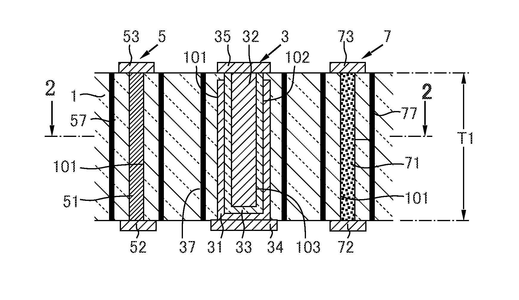
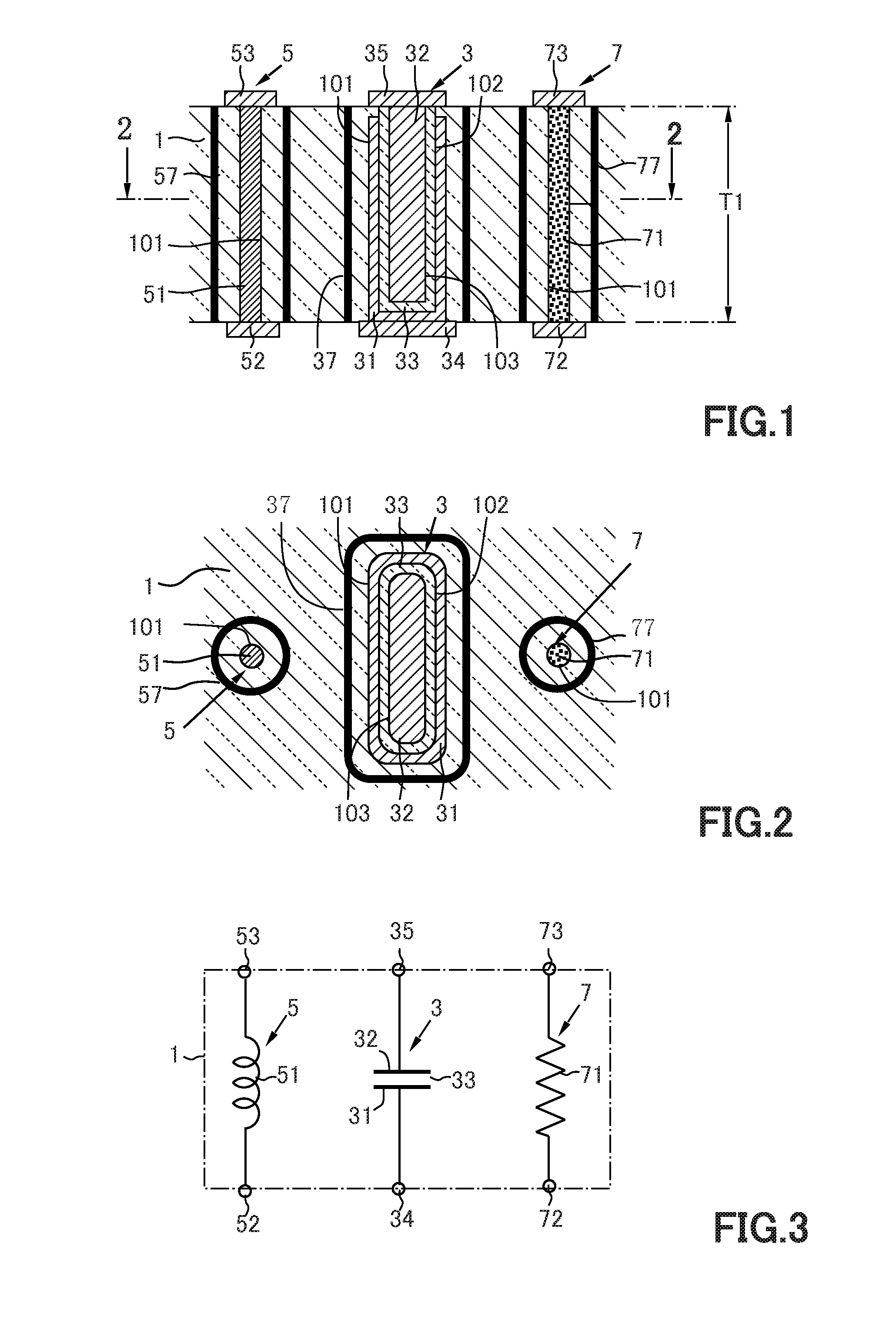
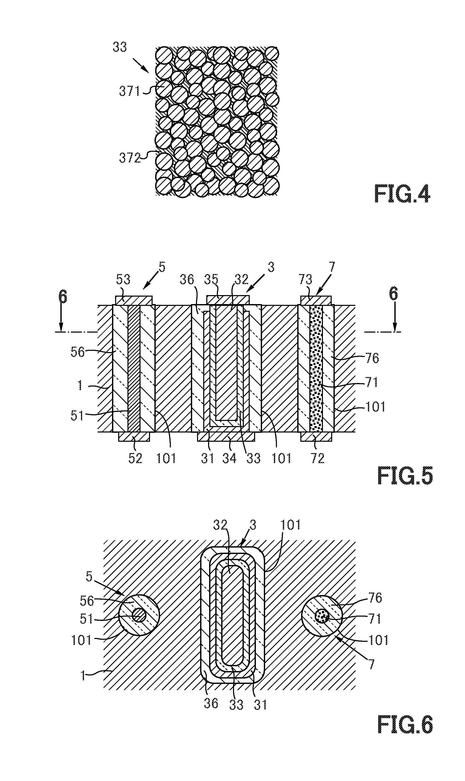
[0055]Referring to FIGS. 1 to 3, a substrate with built-in passive element according to the present invention includes a substrate 1 and passive elements 3, 5 and 7. The substrate 1 has a flat shape with a thickness T1. The substrate 1 may be any of an insulator, a dielectric body, a magnetic body, a semiconductor, a conductor or a combination thereof. Also, it may be an organic substrate, an inorganic substrate or a combination thereof. In this embodiment, for instance, the substrate 1 is an inorganic insulator.

[0056]Typically, the passive elements 3, 5 and 7 may be a capacitor, an inductor, a resistor or a combination thereof. They may also be a signal transmission line or an optical waveguide element. Depending on the type, functional elements of such passive elements include at least one of a conductor, a resistive element, a dielectric element, an insulator, a magnetic element or an optical waveguide. In all embodiments described below, although not shown in the drawings, the s...


PUM


Abstract

A substrate with built-in passive element includes passive elements and a substrate. The passive elements include at least one of a capacitor, an inductor, a resistor, a signal transmission element or an optical waveguide element. The capacitor, the inductor, the resistor, the signal transmission element or the optical waveguide element has a functional element filled in a groove-like or hole-like element forming region provided in the substrate along a thickness direction thereof. The functional element has a Si—O bond region obtained by reacting Si particles with an organic Si compound.

Description

BACKGROUND OF THE INVENTION[0001]1. Field of the Invention The present invention relates to a substrate with built-in passive elements such as a capacitor, an inductor, a resistor, a signal transmission element or an optical waveguide element.[0002]2. Description of the Related Art[0003]In the technical field of electronic component packaging, the 3D packaging is rapidly becoming mainstream instead of the conventional SMT (surface mount technology). Particularly, owing to an increasing demand for miniaturization, high speed and low power consumption, there has been a remarkable progress in the 3D-SiP technology, where the 3D packaging is combined with SiP (system in package) in which a system composed of a plurality of LSIs is enclosed in a single package. The SiP also has an advantage in reducing the power consumption, shorting the development times and reducing the cost. The integration of an advanced system can be achieved by the combination of the SiP and the 3D packaging which ...

Claims


Application Information

Patent Timeline
Patent Type & Authority Applications(United States)
IPC IPC(8): H05K1/18
CPCH05K1/182H01L2924/0002H05K1/0306H05K1/162H05K1/167H05K3/4061H05K2201/086H05K1/165H01L23/481H01L23/5223H01L23/5227H01L23/5228H01L28/10H01L28/20H01L28/40H01L23/535H01L2924/00
Inventor SEKINE, SHIGENOBUSEKINE, YURINAKAMIBAYASHI, KAZUTOSHI
Owner NAPRA
Why Eureka
Try Eureka