Method for reducing charge in critical dimension-scanning electron microscope metrology

a technology of electron microscope and critical dimension, applied in the direction of instruments, semiconductor/solid-state device testing/measurement, non-metal conductors, etc., can solve the problems of gross image distortion or image obliteration, increased inability to accurately measure critical integrated device dimensions in the electronic industry, and increased charging impact, so as to mitigate the charge as a major impact, reduce the charge buildup, and reduce the effect of sem metrology

Inactive Publication Date: 2014-07-24
THE RES FOUND OF STATE UNIV OF NEW YORK +1
View PDF2 Cites 6 Cited by
  • Summary
  • Abstract
  • Description
  • Claims
  • Application Information

AI Technical Summary

Benefits of technology

[0076]One advantage of the present invention is that it provides a method for producing a desired stacked lithographic structure that utilizes the stack as engineered and simply utilizes a silicon under layer, effectively an under layer that comprises a group four element other than Carbon (C).
[0077]An under layer comprising silicon has been previously used in the art as an antireflective coating that can then be used as a hardmask, which is used to define a pattern during etching in an oxygen-containing environment. The inventors have discovered, however, that a silicon-comprising under layer can be used to mitigate charge buildup during SEM metrology. The present invention employs a silicon under layer at extreme ultraviolet (EUV) specifically, and other wavelengths to mitigate charging as a major impact, so that sub-20 nm patterning may be achieved.
[0078]A method is for reducing charge build up is provided comprising the step of coating a layer of imaged photoresist on an under layer (also referred to herein as a bottom coating) comprising silicon, wherein the under layer and the layer of imaged photoresist form two layers of a lithography stack. The under layer renders the photoresist pattern resistant to charging during scanning electron microscopy (SEM). Accumulation of surface charge is known to occur, during CD measurement and inspection lithographically generated patterns, manifesting as gross image distortion and leading to CD measurement error. The method is particularly useful when used on post developed photoresist patterns.
[0079]Since semiconductor patterns are reducing in size, as the industry migrates to EUV lithography, tighter pattern density creates microenvironment where electron charge concentrates. Utilizing the spin-able film stack disclosed herein is a cost-effective solution to controlling measurement the error caused by charging.
[0080]In one embodiment, a structure with at least one CD of interest is built on a under layer comprising silicon using successive (or reiterative) lithographic process steps. Such lithographic steps are known in the art, and the same lithography step can be performed repeatedly to create a layered device (wafer). The reduction or elimination of charge buildup allows much enhanced resolution and accurate measurements of CDs.
[0081]In a preferred embodiment, extreme ultraviolet lithography (EUVL) is employed to construct an integrated circuit or integrated device, and the silicon-comprising under layer is used to mitigate charge accumulation and its detrimental impact on SEM metrology. EUVL methods are known in the art.

Problems solved by technology

A major problem in using SEM for metrology of CDs is that as the target feature size decreases, the impact of charging increases.
The buildup of surface charge on a specimen caused by the electron beam of the SEM will thus cause gross image distortion or image obliteration.
Such image distortion or obliteration has led to an increasing inability to accurately measure critical integrated device dimensions in the electronic industry.
Since CDs are becoming increasingly smaller as lithographic technology advances, such inaccuracies pose a significant problem in the manufacture of integrated circuits.

Method used


Image

  • Method for reducing charge in critical dimension-scanning electron microscope metrology
  • Method for reducing charge in critical dimension-scanning electron microscope metrology
  • Method for reducing charge in critical dimension-scanning electron microscope metrology

Examples


example 1

6.1. Example 1

Charging of Extreme Ultraviolet (EUV) Photoresist Targets in Critical Dimension Scanning Electron Microscopy (CD-SEM)

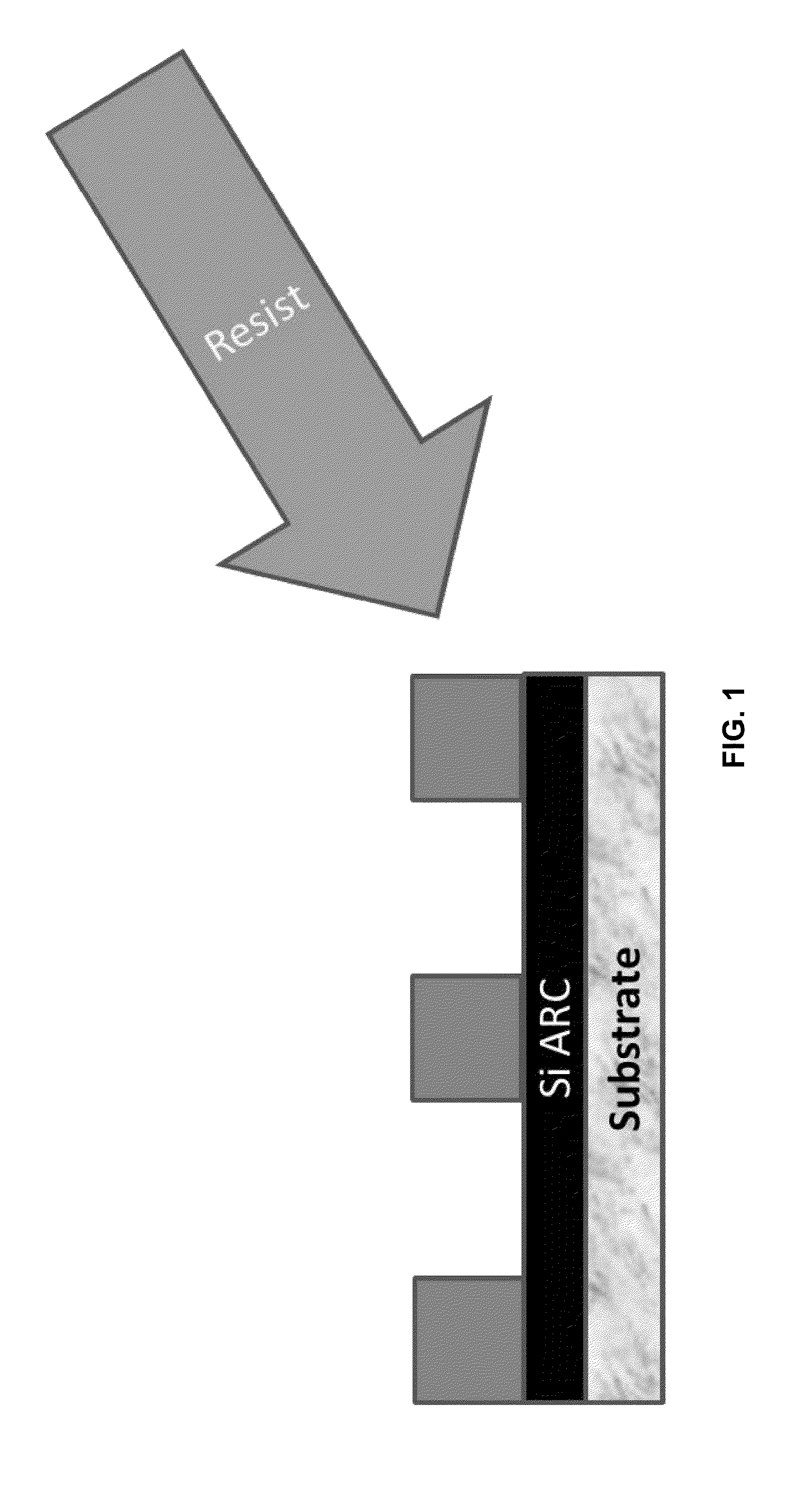
[0114]This example demonstrates that a silicon-comprising coating can be applied as a film to coat a photoresist sample to mitigate sample charging. The SiARC SHBA 940 (Shin Etsu, Tokyo, Japan) is typically used as a hardmask for tri-layer image processing and to define patterns in organic films via O2 plasma etching (Wei, Yet al. 2011. Proc. SPIE 7972, 79722L (2011). According to techniques currently practiced in the art, discharge layers can be coated on top of the imaging layer of a photoresist prior to electron beam exposure to help reduce or eliminate the charge build up that deflects the electron beam during exposure. The discharge layers, however, do not contain silicon nor have they been applied under a photoresist layer for the purpose of mitigating charging. This example shows that using SiARC as an underlayer for sub-30 nm photoresist images r...

example 2

6.2. Example 2

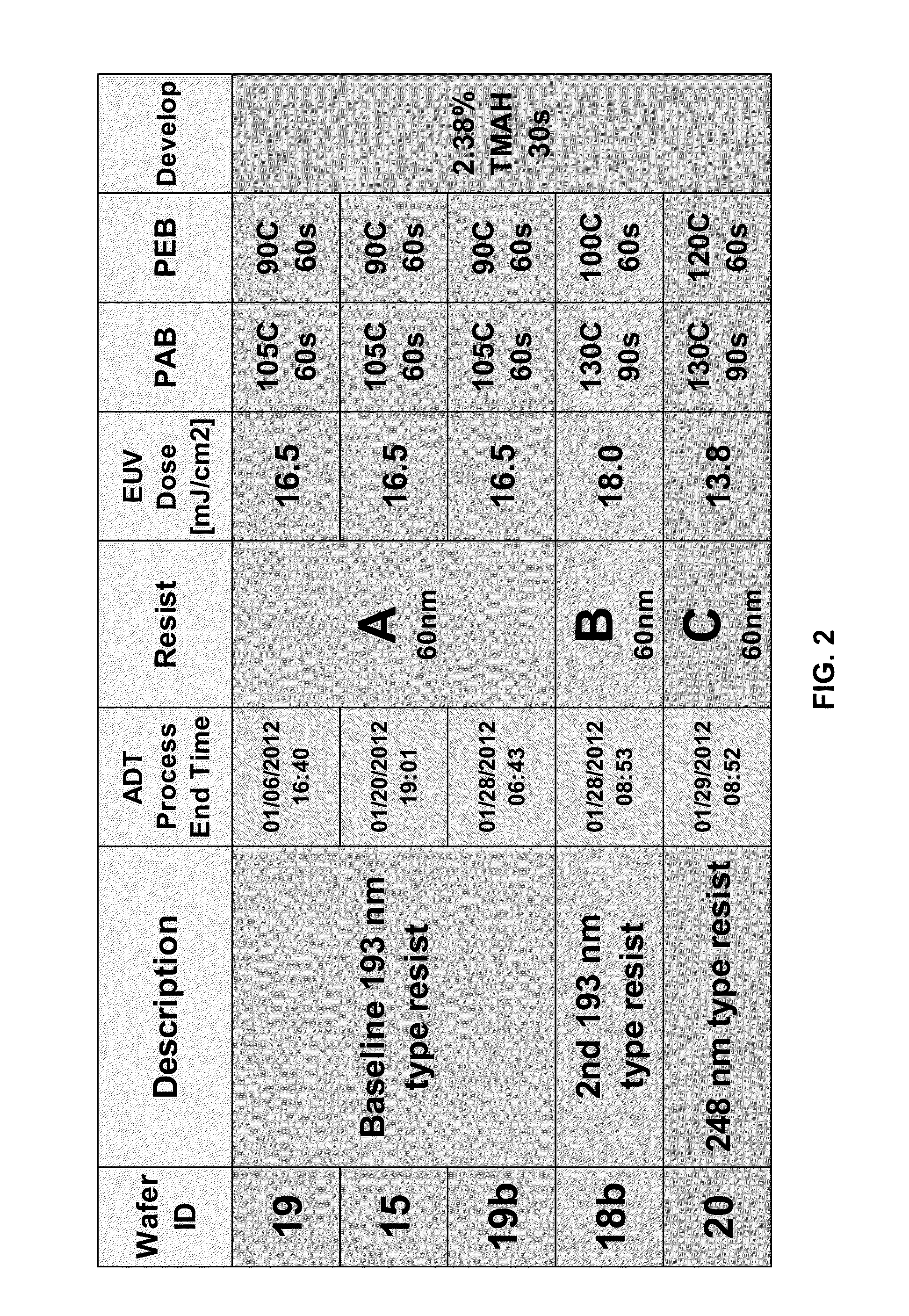
SEM Metrology of Photoresist Shrinkage in EUV Lithography of an Integrated Circuit

[0127]Charge build up is an important systematic uncertainty source in critical dimension-scanning electron microscope (CD-SEM) metrology of lithographic features. In terms of metrology gauge metrics, it influences both the precision and the accuracy of CD-SEM measurements. Minimization or elimination of charge build up is desirable, yet elusive. This error source plays a significant role in the accuracy of CD-SEM metrology on polymer materials, especially as EUV lithography (EUVL) becomes a preferred lithographic method for producing integrated circuits.

[0128]In this example, a silicon-comprising under layer, a silicon-comprising under layer comprising a SiARC (SHBA 940, Shin Etsu, Tokyo, Japan) is used to reduce charge buildup during CD-SEM metrology of static and dynamic shrinkage behaviors of various EUV photoresists. The use of the silicon-comprising under layer decreases charge buil...


PUM

PropertyMeasurementUnit
wavelengthsaaaaaaaaaa
wavelengthaaaaaaaaaa
thickaaaaaaaaaa

Abstract

Methods and compositions are provided for reducing or eliminating charge buildup during scanning electron microscopy (SEM) metrology of a critical dimension (CD) in a structure produced by lithography. An under layer is utilized that comprises silicon in the construction of the structure. When the lithography structure comprising the silicon-comprising under layer is scanned for CDs using SEM, the under layer reduces or eliminates charge buildup during SEM metrological observations.

Description

CROSS-REFERENCE TO RELATED APPLICATIONS[0001]This application claims priority to and the benefit of co-pending U.S. provisional patent application Ser. No. 61 / 754,148, entitled Method For Reducing Charge in Critical Dimension-Scanning Electron Microscope Metrology, filed Jan. 18, 2013, which is incorporated herein by reference in its entirety.1. TECHNICAL FIELD[0002]The present invention relates to methods and compositions for reducing charge buildup and improving the accuracy of measurement in critical dimension-scanning electron microscope (CD-SEM) metrology. The invention also relates to methods and compositions for constructing integrated circuits or devices that can be more accurately or precisely measured by CD-SEM metrology.2. BACKGROUND OF THE INVENTION[0003]Measurement and inspection of critical dimensions (CDs) of lithographically patterned features produced in the manufacture of integrated circuits utilizes scanning electron microscopy (SEM) to determine whether target pa...

Claims


Application Information

Patent Timeline
Patent Type & Authority Applications(United States)
IPC IPC(8): H01L21/66H01L21/033
CPCH01L21/0337H01L22/12G03F7/075G03F7/091G01B15/00G01B2210/56G01N23/2251G01N2223/6116G03F7/0752G03F7/0757G03F7/2004H01L21/0276
Inventor MONTGOMERY, MELVIN WARRENMONTGOMERY, CECILIA ANNETTEBUNDAY, BENJAMIN D.
Owner THE RES FOUND OF STATE UNIV OF NEW YORK
Why Eureka
Try Eureka