Semiconductor light-emitting device and method of manufacturing the same

a technology of semiconductor light-emitting devices and manufacturing methods, which is applied in the direction of semiconductor devices, basic electric elements, electrical appliances, etc., can solve the problems of affecting the device performance, affecting the light generation efficiency, and forming defects of misfit dislocation in the vicinity, so as to reduce the risk of stress and heat building up in the device structure, the effect of reducing the risk of substrate stress and hea

Active Publication Date: 2014-08-21
WANG TIEN YANG
View PDF2 Cites 13 Cited by
  • Summary
  • Abstract
  • Description
  • Claims
  • Application Information

AI Technical Summary

Benefits of technology

[0005]The present light emitting device can overcome aforementioned deficiencies. The present invention may include one or more of the following advantages. The adverse influence of the substrate on device performance is reduced in the present device. The defect level is lower and there is a less chance for stress and heat to build up in the device structure. The light absorption loss is less and the extraction efficiency is improved in the present device. The present device may be processed without damaging the device layer. The light emitting structure may be configured in a pattern for desirable beam profile of the present device. The burden of resorting to sophisticated lens design to match the optics of the luminaries may be relaxed. The present device may emit lights in multiple colors. The present device may generate a white light emission for use in general lighting and display systems.
[0006]One objective of the present invention relates in general to defect reduction in device. In specific, to reduce dislocation defects in LED device due to lattice mismatch between layer and the substrate. Another objective of the present invention relates in general to the shaping of the beam profile of the LED device. In specific, beam shaping is realized by forming the LED structure in a pattern rather than etching the chip. A further objective of the present invention relates in general to a high efficiency LED that may be manufactured in a manner more compatible with the established cost-effective processing and packaging methods for large size wafers from the IC industry. This would further reduce the cost of ownership ($ / lumen) in LED systems for lighting and display backlight applications.

Problems solved by technology

There are several issues in the conventional device.
This is accompanied by the formation of misfit dislocation defects in the vicinity of the substrate interface.
This would impair the light generation efficiency of the LED and adversely affect the performance of the device.
The situation becomes worse in the GaN / Si materials system, which exhibits a lattice mismatch of 17% and a thermal mismatch of +100% between the GaN layer and the Si substrate wafer.
In this case, the relaxation of the excessive strain energy often leads to the formation of micro cracks making the device inoperative.
There are drawbacks in the prior art methods.
However, the layer growth through a slit is less predictable due to the difficulty of fast switching of source nutrients within the narrow space confined in the channel.
Moreover, the build up of thermal stress in the overgrowing layer that adheres intimately to the mask would cause layer distortion and generation of extra defects.
However, it remains a challenge to maintain a uniform etching profile across the substrate surface.
The situation gets worse as the wafer size increases.

Method used


Image

  • Semiconductor light-emitting device and method of manufacturing the same
  • Semiconductor light-emitting device and method of manufacturing the same
  • Semiconductor light-emitting device and method of manufacturing the same

Examples


Embodiment Construction

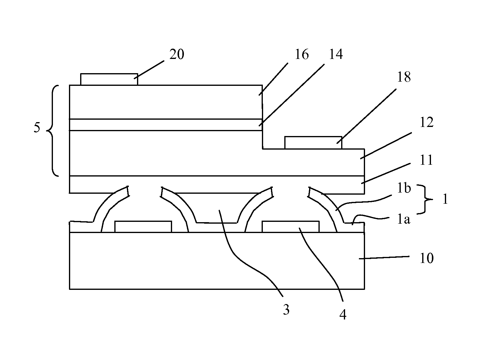
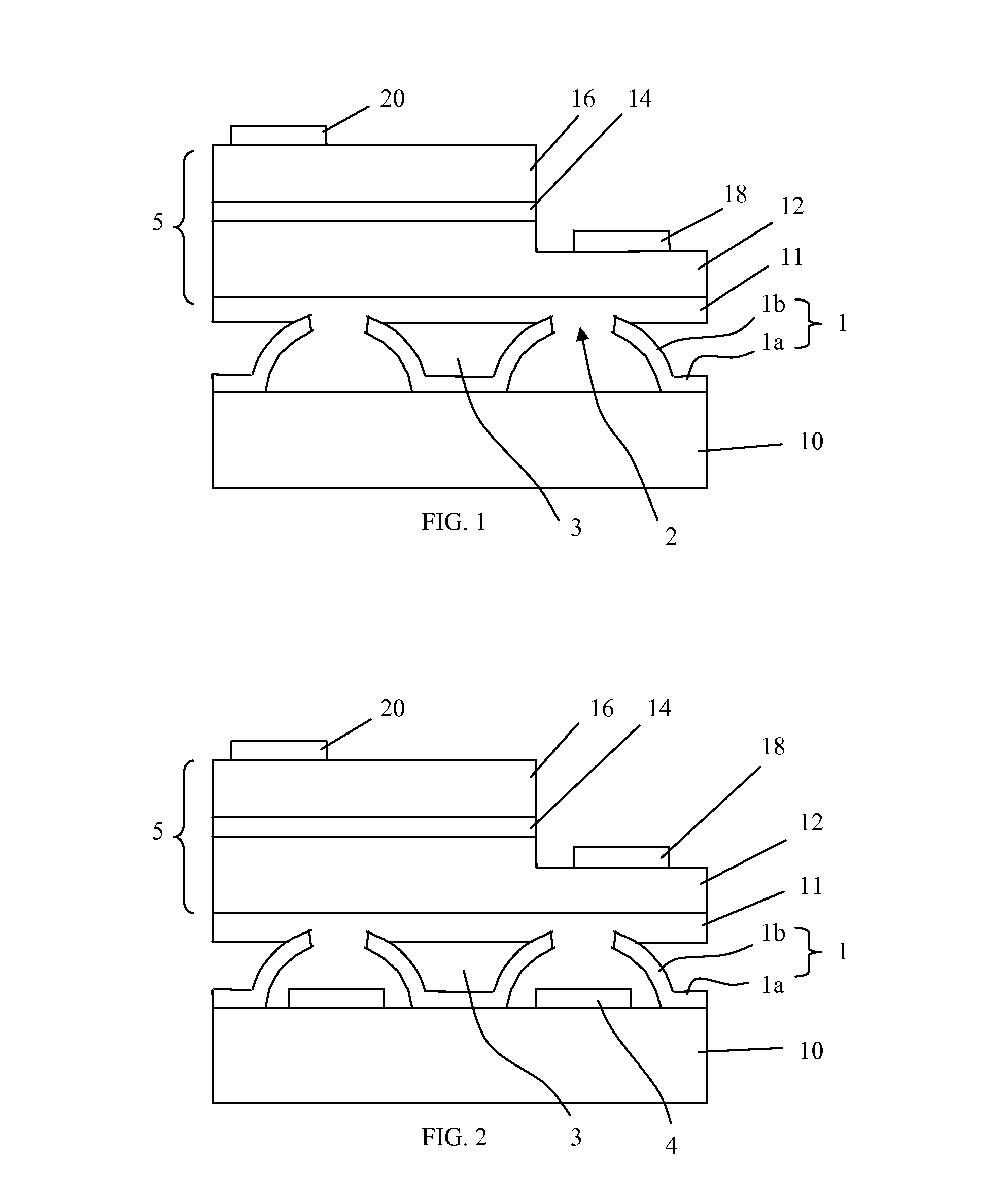
[0030]FIG. 1 is a simplified, cross sectional view of an illustrative example of the light emitting device in an embodiment of the present invention. The light emitting device may comprise a light emitting structure that is formed using layer deposition. In this example, the light emitting structure 5 may comprise a lower layer of the first conductivity type 12, an active layer 14, an upper layer of the second conductivity type 16. The light emitting device may further comprise a first electrode 18 connected to the lower layer of the first conductivity type; a second electrode 20 connected to the upper layer of the second conductivity type. The light emitting structure 5 may comprise a variety of materials selected from the group comprising III-V materials, group IV, group II-VI semiconductor materials. Suitable substrates may include the group III-V, group IV, group II-VI elements, alloys, oxides such as ZnO, spinel, and sapphire. In the present device, the light emitting structure...


PUM


Abstract

A light-emitting device is disclosed including a light emitting structure comprising a lower layer of the first conductivity type, an active layer, an upper layer of the second conductivity type; a first electrode connected to the lower layer of the first conductivity type; a second electrode connected to the upper layer of the second conductivity type. The light emitting structure is formed using a shell member, which comprises a planar portion and a shell portion. The extent of growth defects such as misfit dislocations is reduced and the extraction of light and heat is improved in the present device. The beam profile of the device may be altered by patterning the light emitting structure instead of shaping the entire chip. The device may be manufactured in a way more compatible with the established, cost-effective processing and packaging methods for large size wafers from the IC industry.

Description

BACKGROUND OF THE INVENTION[0001]The present invention relates in general to the fabrication of semiconductor light emitting devices (LED), and in particular, to an LED with improved luminance efficiency.[0002]In a conventional LED, the light emitting structures is disposed on the surface of a substrate wafer comprising an active region sandwiched between upper and lower layer of opposite conductivity. The active region may contain multiple quantum wells (MQW) comprising alternating barrier layer and well layer to improve light generation efficiency. A blocking layer is also preferably included adjacent to the MQW to reduce the carrier leakage. In a GaN LED for example, the MQW contains GaN barrier layers and InGaN well layers in a blue LED. Typical substrates in the production of GaN LED are sapphire, SiC and Si. There are several issues in the conventional device. For example, there is a significant lattice mismatch of 13% and a thermal mismatch of −34% between GaN layer and sapph...

Claims


Application Information

Patent Timeline
Patent Type & Authority Applications(United States)
IPC IPC(8): H01L33/12
CPCH01L33/12H01L27/156H01L33/20H01L33/60H01L2924/0002
Inventor WANG, TIEN YANG
Owner WANG TIEN YANG
Why Eureka
Try Eureka