

Semiconductor device
- Summary
- Abstract
- Description
- Claims
- Application Information
AI Technical Summary
Benefits of technology
Problems solved by technology
Method used
Image

Examples
first embodiment
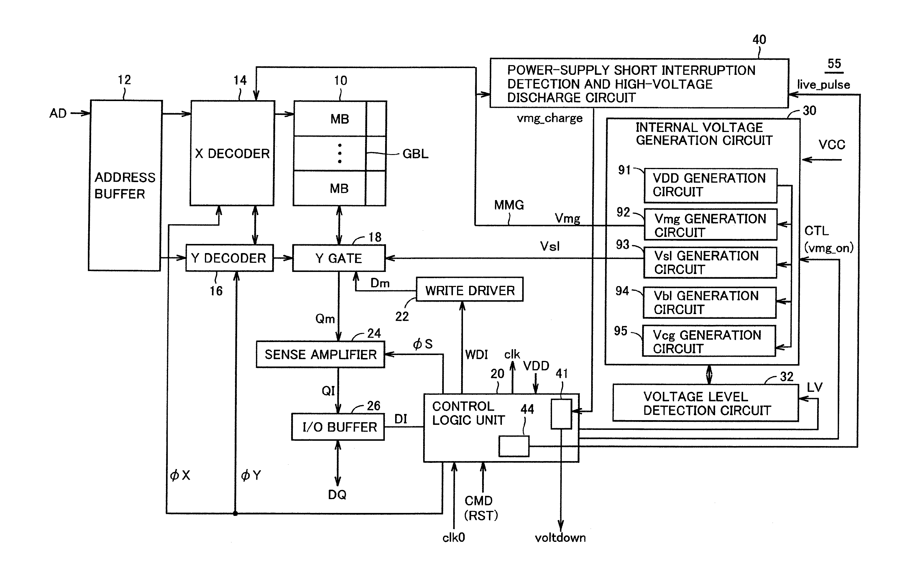
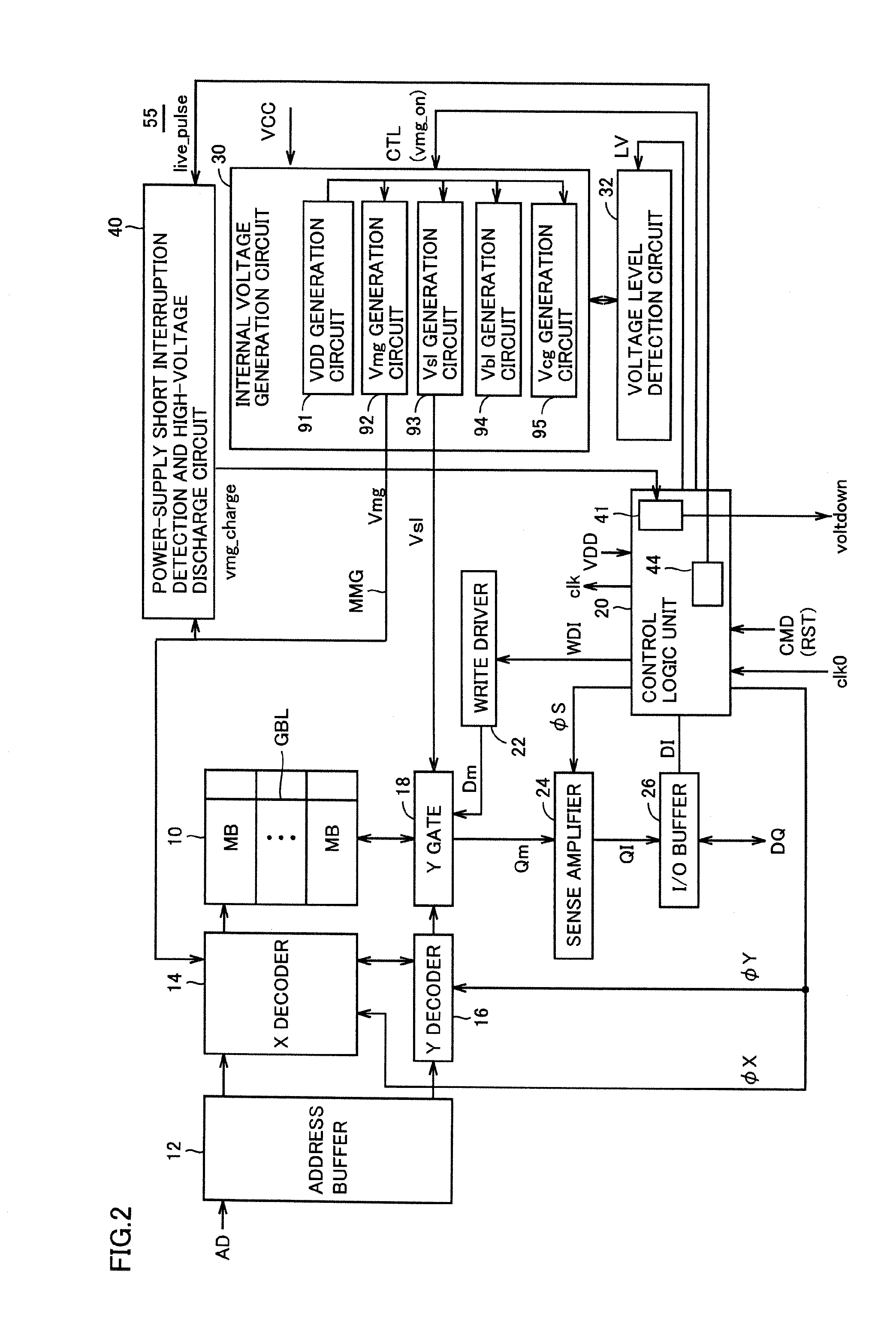
[0026]Microcomputer
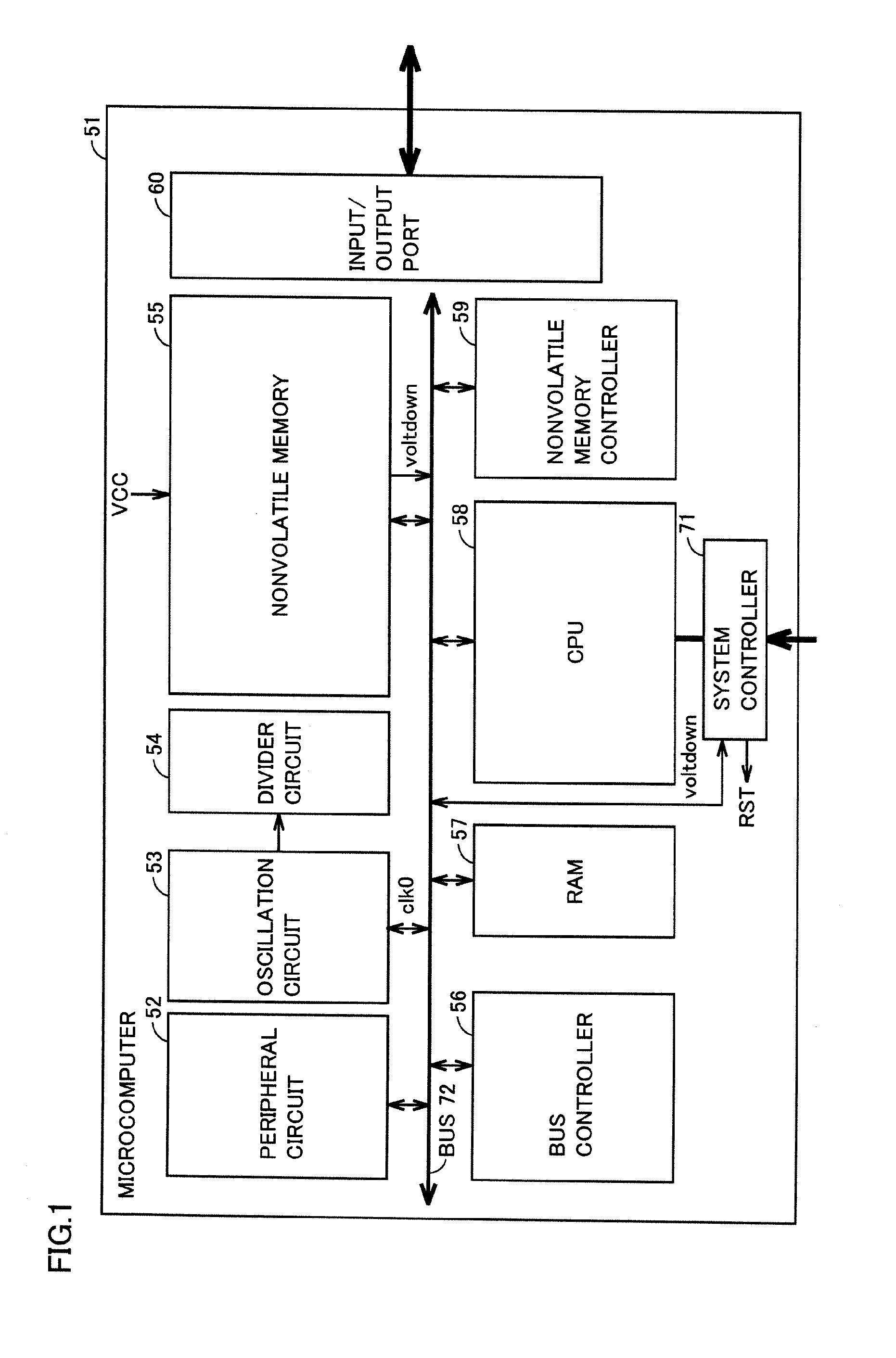
[0027]FIG. 1 is a configuration diagram of a microcomputer provided with a nonvolatile semiconductor memory in an embodiment of the present invention.
[0028]Microcomputer 51 includes a peripheral circuit 52, an oscillation circuit 53 generating reference clock clk0, a divider circuit 54 dividing reference clock clk0 generated by oscillation circuit 53, a bus controller 56 controlling transmission of a signal passed through a bus 72, a RAM (Random Access Memory) 57, a CPU 58, and a system controller 71 controlling the overall operation of microcomputer 51. Microcomputer 51 further includes a nonvolatile semiconductor memory 55, a nonvolatile semiconductor memory controller 59 controlling writing to the nonvolatile semiconductor memory in accordance with an instruction from CPU 58, and an input / output port 60 which outputs a signal to external circuitry and receives a signal from external circuitry.
[0029]When nonvolatile semiconductor memory 55 detects short interrup...
second embodiment
[0100]In the first embodiment, a periodic one-shot pulse is used as control signal live_pulse. Control signal live_pulse applied to first discharge circuit 82, however, may be any signal as long as the signal is activated to “H” level when short interruption of an internal power supply does not occur and inactivated to “L” level upon occurrence of short interruption of the internal power supply. The present embodiment provides another example of control signal live_pulse whose level is changed in the aforementioned manner.
[0101]Discharge Control Unit
[0102]FIG. 12 is a diagram showing a configuration of a discharge control unit 44 in a second embodiment.
[0103]As shown in FIG. 12, discharge control unit 44 includes a plurality of flip-flops 61_1 to 61_N, and a logical product circuit 62 which outputs a logical product of respective outputs of a plurality of flip-flops 61_1 to 61_N. A MOS transistor which is a component in at least one flip-flop of these flip flops 61_1 to 61_N has a s...
PUM
 Abstract
Description
Claims
Application Information