
Superconducting Single Photon Detector

a single-photon detector and superconducting technology, applied in the direction of photometry using electric radiation detectors, optical radiation measurement, instruments, etc., can solve the problems of imperfect detector characteristics, limited rate and range of quantum key distribution implementations, 145-195), and limit the usefulness of large-scale integrated photon counting applications

Active Publication Date: 2014-10-09
YALE UNIV
View PDF2 Cites 99 Cited by
  • Summary
  • Abstract
  • Description
  • Claims
  • Application Information

AI Technical Summary

Benefits of technology

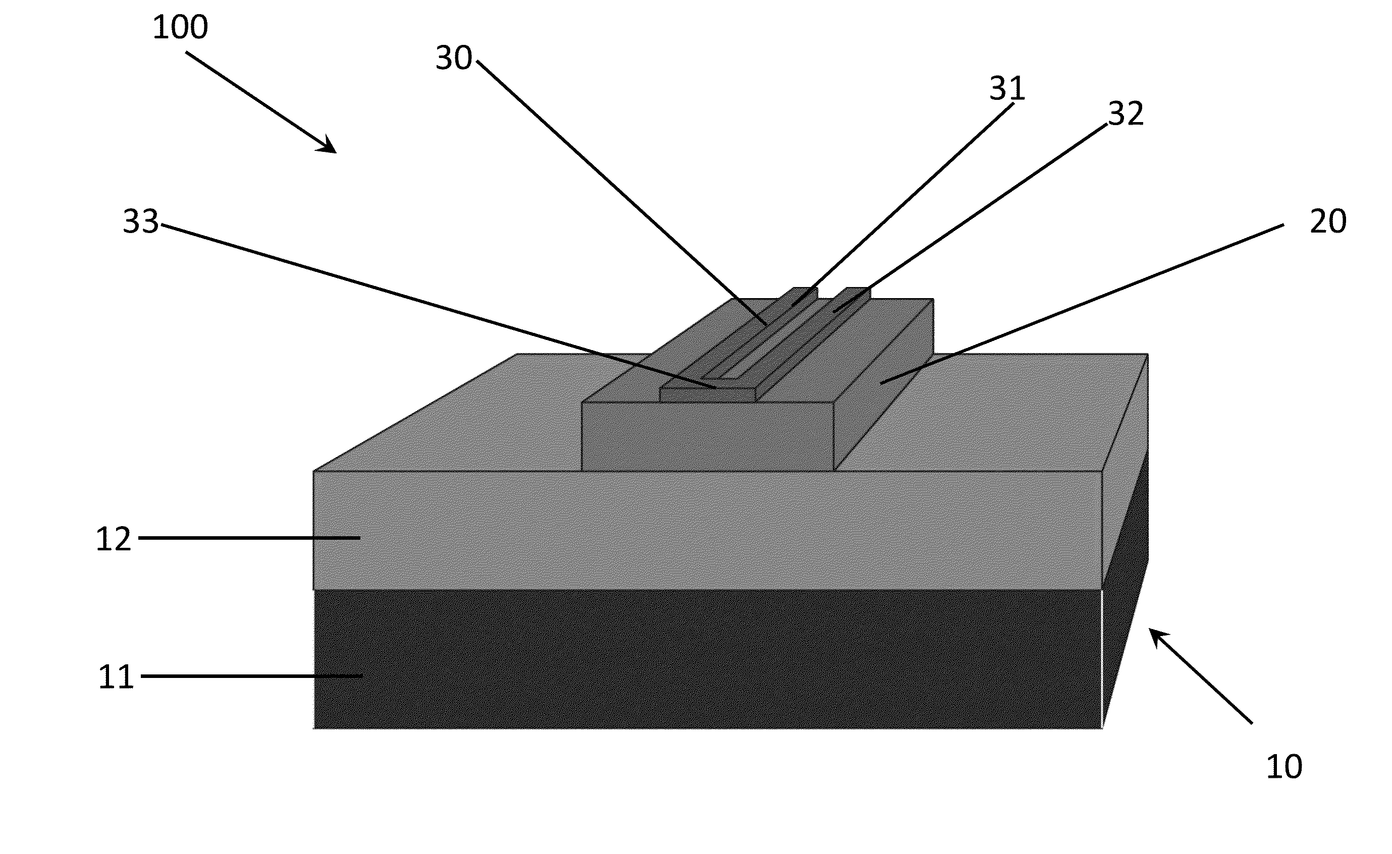
The present invention is about a device and system for detecting single photons in the visible and infrared spectrum. The device includes a waveguide layer and a superconducting nanowire positioned atop of the waveguide layer. The nanowire can be made of various materials such as silicon nitride, aluminum nitride, gallium nitride, sapphire, diamond, silicon, gallium phosphide, silicon oxide, and magnesium oxide. The device can be integrated within a photonic chip and can be housed within a cryostat. The technical effects of the invention include improved detection of single photons, reduced dark current, and improved signal-to-noise ratios.

Problems solved by technology

Most prominently, quantum key distribution implementations (Takesue et al., 2007, Nat. Photon., 1(6): 343-348; Gisin et al., 2002, Rev. Mod. Phys., 74(1): 145-195) are currently limited in rate and range by imperfect detector characteristics.
These types of devices limit their usefulness for large scale integrated photon counting applications.
While the compatibility of quantum waveguide circuits and SSPDs has been successfully demonstrated (Natarajan et al., 2010, Appl. Phys. Lett., 96(21): 211101-1-211101-3), the coupling of photons from a chip to a separate detector limits the performance of this approach.

Method used


Image

  • Superconducting Single Photon Detector
  • Superconducting Single Photon Detector
  • Superconducting Single Photon Detector

Examples


experimental examples

[0077]The invention is further described in detail by reference to the following experimental examples. These examples are provided for purposes of illustration only, and are not intended to be limiting unless otherwise specified. Thus, the invention should in no way be construed as being limited to the following examples, but rather, should be construed to encompass any and all variations which become evident as a result of the teaching provided herein.

[0078]Without further description, it is believed that one of ordinary skill in the art can, using the preceding description and the following illustrative examples, make and utilize the present invention and practice the claimed methods. The following working examples therefore, specifically point out the preferred embodiments of the present invention, and are not to be construed as limiting in any way the remainder of the disclosure.

example 1

NbTiN Superconducting Nanowire Detectors for Visible and Telecom Wavelengths Single Photon Counting on Si3N4 Photonic Circuits

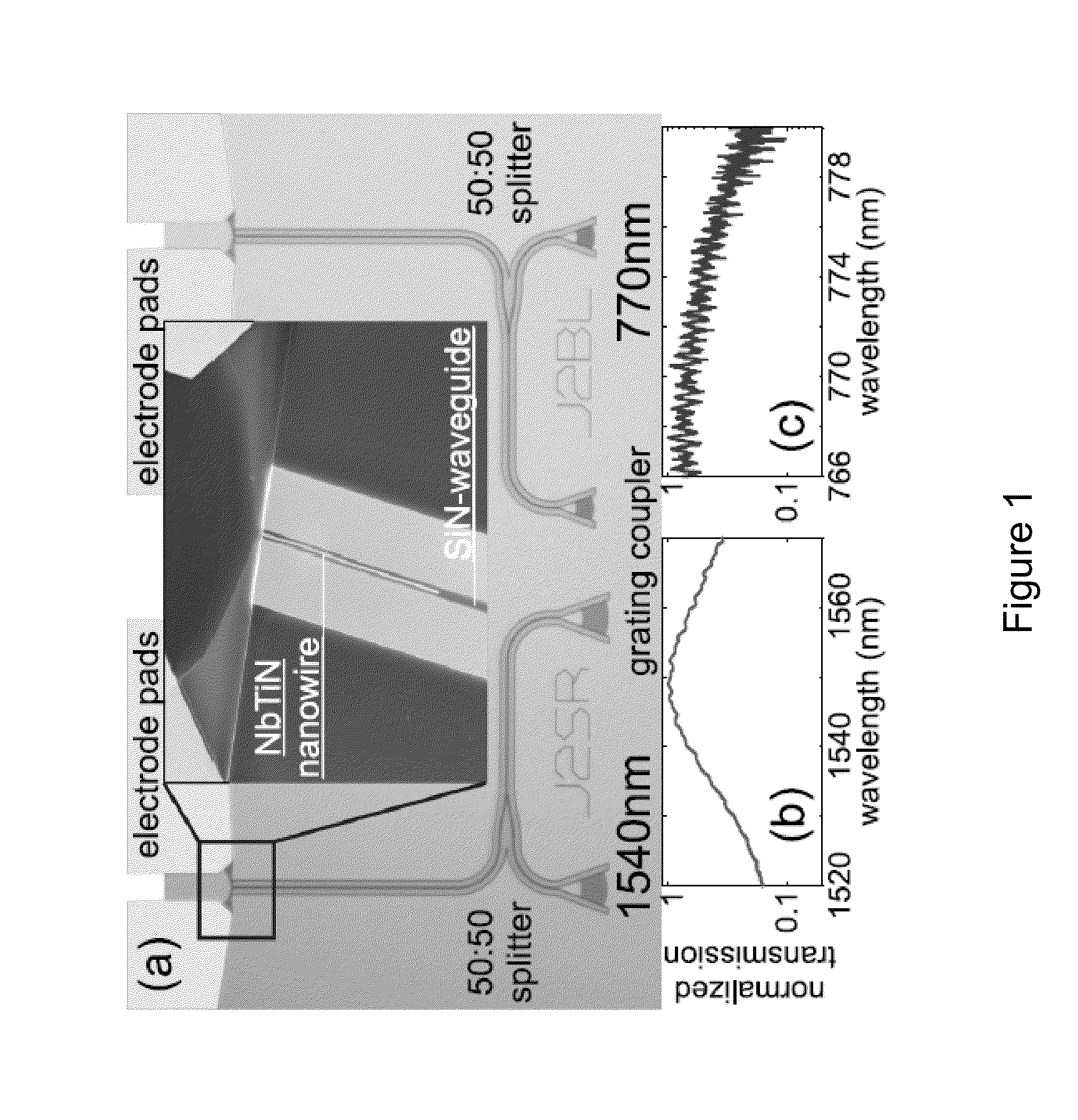
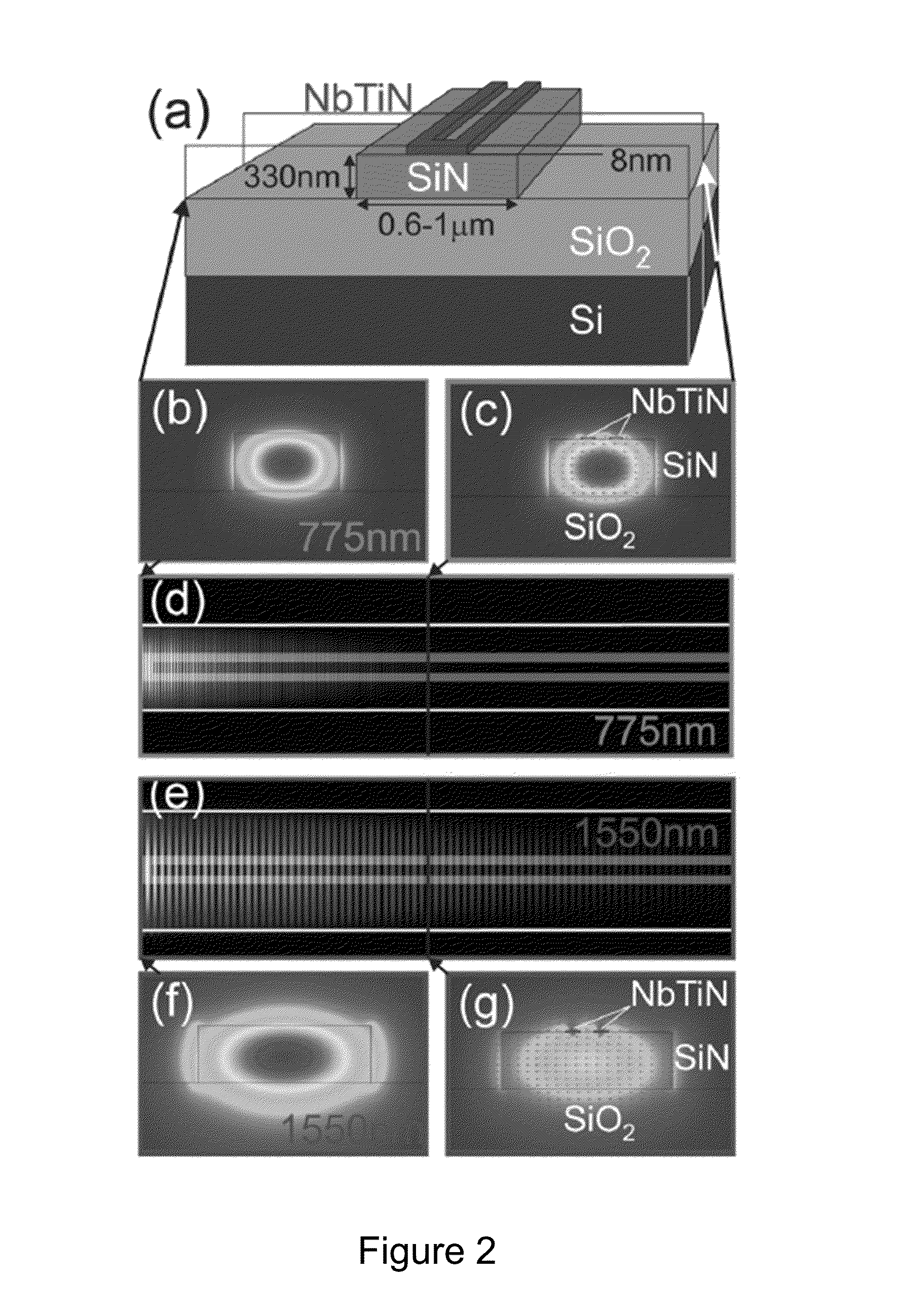
[0079]Described herein is the demonstration of niobium titanium nitride (NbTiN) superconducting nanowires patterned on stoichiometric silicon nitride waveguides for detecting visible and infrared photons. The use of silicon nitride on insulator on silicon substrates allows for the simultaneously realization of photonic circuits for visible and infrared light and the integration of such circuits with nanowire detectors directly on-chip. By implementing a traveling wave detector geometry in this material platform, efficient single photon detection is achieved for both wavelength regimes. The waveguide coupled SSPDs presented here is a development primarily addressing the needs of integrated photonics and quantum information processing (Pernice et al., 2012, Nat. Commun., 3: 1325; Sprengers et al., 2011, Appl. Phys. Lett., 99: 181110). The described detectors ar...

example 2

Waveguide Integrated Low Noise NbTiN Nanowire Single-Photon Detectors with Milli-Hz Dark Count Rate

[0090]Superconducting nanowire single-photon detectors are an ideal match for integrated quantum photonic circuits due to their high detection efficiency for telecom wavelength photons. Quantum optical technology also requires single-photon detection with low dark count rate and high timing accuracy. Presented herein are very low noise superconducting nanowire single-photon detectors based on NbTiN thin films patterned directly on top of Si3N4 waveguides. A large variety of detector designs are systematically investigated and their detection noise performance is characterized. Milli-Hz dark count rates are demonstrated over the entire operating range of the nanowire detectors which also feature low timing jitter. The ultra-low dark count rate, in combination with the high detection efficiency inherent to the travelling wave detector geometry, gives rise to a measured noise equivalent p...


PUM


Abstract

The present invention provides a device and system for high-efficiency and low-noise detection of single photons within the visible and infrared spectrum. In certain embodiments, the device of the invention can be integrated within photonic circuits to provide on-chip photon detection. The device comprises a traveling wave design comprising a waveguide layer and a superconducting nanowire atop of the waveguide.

Description

CROSS-REFERENCE TO RELATED APPLICATIONS[0001]This application claims priority to U.S. Provisional Application Ser. No. 61 / 732,500, filed Dec. 3, 2012, the contents of which are incorporated by reference herein in their entiretySTATEMENT REGARDING FEDERALLY SPONSORED RESEARCH OR DEVELOPMENT[0002]This invention was made with government support under 0846919 awarded by the National Science Foundation. The government has certain rights in the invention.BACKGROUND OF THE INVENTION[0003]Low dark count rate, high detection efficiency and accurate timing resolution are the three most desired features of a single-photon detector (Hadfield, 2009, Nat. Photon., 3(12): 696-705; Eisaman et al., 2011, Rev. Sci. Instrum., 82(7): 071101) These characteristics can be combined to one figure-of-merit for single-photon detectors, for example the noise equivalent power (NEP). Detectors with low noise performances are increasingly sought after for applications in both quantum and classical technology. In...

Claims


Application Information

Patent Timeline
Patent Type & Authority Applications(United States)
IPC IPC(8): G01J1/04G02B6/02G02B6/12
CPCG01J1/0425G02B6/12B82Y20/00Y10S977/954G02B6/0229G01J2001/442G02B6/12004
Inventor TANG, HONGXINGPERNICE, WOLFRAMSCHUCK, CARSTEN
Owner YALE UNIV
Learn More