

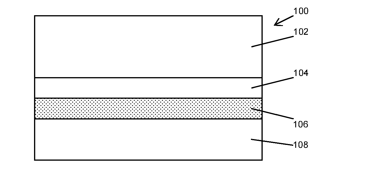
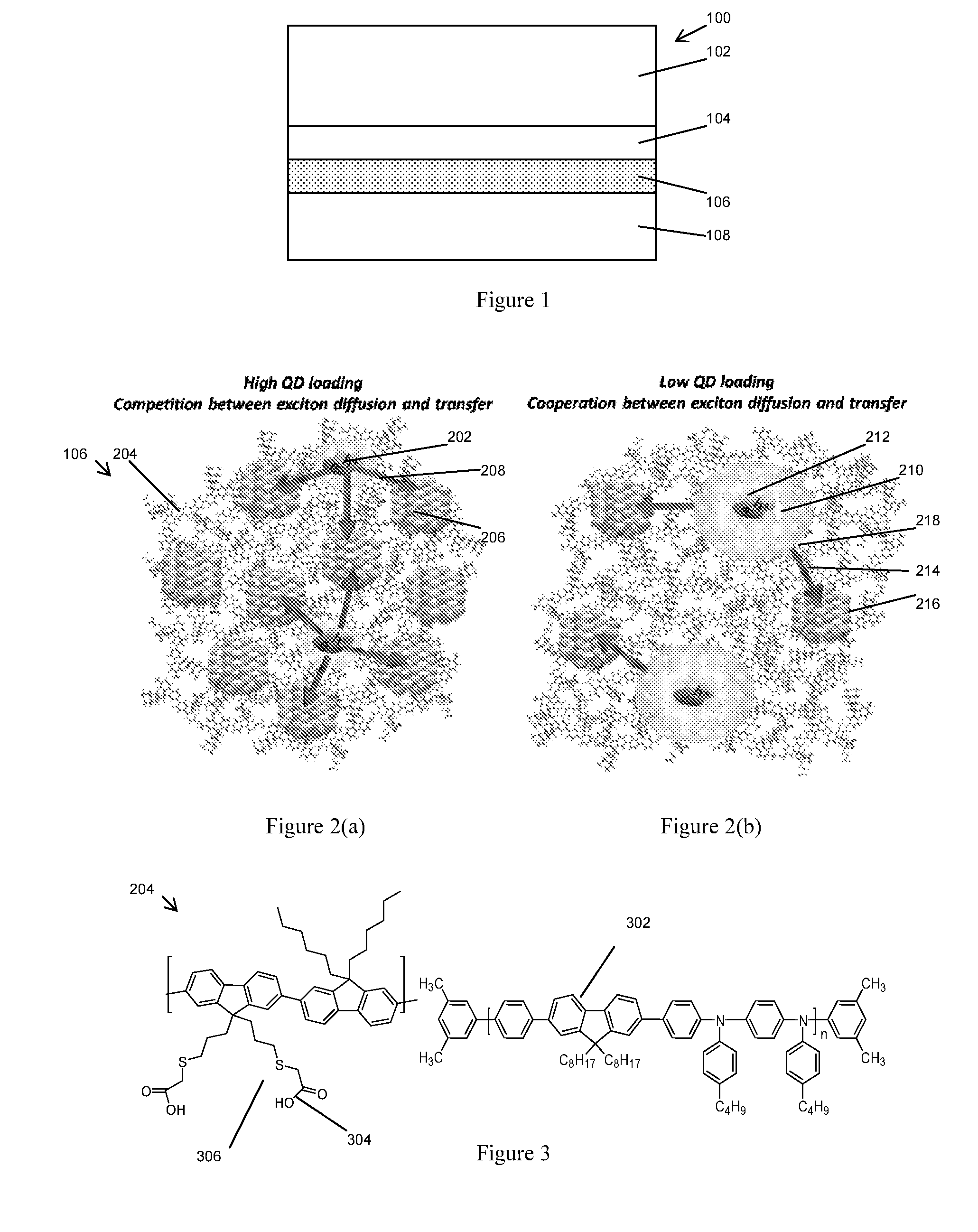
Light-emitting device
a light-emitting device and light-emitting diode technology, applied in semiconductor devices, solid-state devices, nanotechnology, etc., can solve the problems of weak charge injection and transport across the nqd thin film, poor nret efficiency, and failure of nret-based quantum well led to date, and achieve high loading
- Summary
- Abstract
- Description
- Claims
- Application Information
AI Technical Summary
Benefits of technology
Problems solved by technology
Method used
Image

Examples
example 1
[0089]The synthesis procedure for NQDs described in Lim et al.17 is incorporated herein by reference.
Film preparation
[0090]Double side polished quartz substrates were cleaned using multiple solvents (detergent, water, acetone and isopropanol). 20 mg / mL of functionalised PF in THF and 10 mg / mL of CdSe / CdS / ZnS NQD solution in toluene were mixed and stirred with sonication. Subsequently, the mixture was spin-coated at 2000 rpm for 1.5 min. The resulting thin film thickness was measured to be 60 nm using a profilometer.
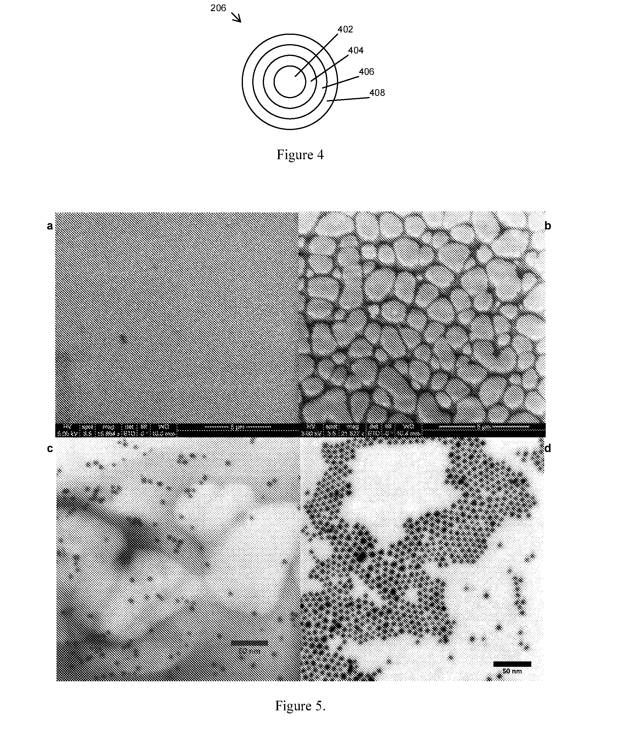
EM and TEM Characterizations
[0091]Scanning electron microscopy (Quanta 200 FEG, FEI) of the hybrid and blend films spin-coated on (100) p-doped silicon substrates was carried out. Energy dispersive X-ray spectrometer integrated with our SEM system (EDAX, Materials Analysis Division) was used to understand the phase segregated parts of the films. Transmission electron microscopy (Technai G2 F30, FEI) was used with ultra thin carbon grids in scanning mode via high sensitivi...
PUM
| Property | Measurement | Unit |
|---|---|---|
| thickness | aaaaa | aaaaa |
| diffusion length | aaaaa | aaaaa |
| diffusion length | aaaaa | aaaaa |
Abstract
Description
Claims
Application Information