Sintering Metallic Inks on Low Melting Point Substrates

a technology of metallic inks and substrates, applied in the direction of semiconductors, nuclear engineering, electrical engineering, etc., can solve the problems of high energy consumption, high cost, and high cost of sintering copper inks or paste films applied to low melting point flexible films, etc., to achieve the effect of reducing the overall density and conductivity of the film, increasing the adhesion between adjacent particles, and increasing the adhesion of inks

Inactive Publication Date: 2014-10-23
APPLIED NANOTECH HLDG
View PDF3 Cites 13 Cited by
  • Summary
  • Abstract
  • Description
  • Claims
  • Application Information

AI Technical Summary

Benefits of technology

[0009]Placing a binder material in the ink increases the adhesion between adjacent particles within the film. Binder in the ink can increase the adhesion of the ink to the substrate but at the expense of film conductivity. Binder should be removed from the interface between the particles in the turn or they cannot connect to form conductive pathways. If not completely removed, the residue will reduce the overall density and conductivity of the film.

Problems solved by technology

Sintering copper ink or paste films applied to low melting point flexible films (e.g., PET, PEN), is problematic, since the substrate material would be thermally damaged at typical copper sintering temperatures.
The process of energy conversion can be considered rapid and violent with respect to the energy level of the nanoparticles.
Determining the correct parameters to obtain a sintered, continuous, copper film, with photonic “flash lamp” sintering, is very difficult due to the cracking and “blow off” of the ink or paste film prevalent with such a process.
There is a significant market interest for conductive metallic films / features / devices on lower cost flexible films, such as those made with polyethylene terephthalate (PET However, due to film temperature exposure limits, and poor adhesion with “flash lamp” high energy pulsed light sintering.
PET is a difficult film to work with.
Routinely, efforts to use a “flash lamp” to cure a copper ink film coated onto a PET substrate or film resulted in non-conductive films.
The cured film would crack, and most commonly, would ablate or “blow off” due to severe cracking and poor adhesion to the film.
However, due to the small size and mass of the individual particles, it is easy to overwhelm the energy requirements and quickly put too much energy into the film.
If the energy delivery is too fast or too intense, the intraparticle mass transfer cannot keep up with the internal mechanisms to shed heat.
These processes can take seconds to hours to complete depending on the particular adhesive interface.
Binder in the ink can increase the adhesion of the ink to the substrate but at the expense of film conductivity.
If not completely removed, the residue will reduce the overall density and conductivity of the film.

Method used


Image

  • Sintering Metallic Inks on Low Melting Point Substrates
  • Sintering Metallic Inks on Low Melting Point Substrates
  • Sintering Metallic Inks on Low Melting Point Substrates

Examples


Embodiment Construction

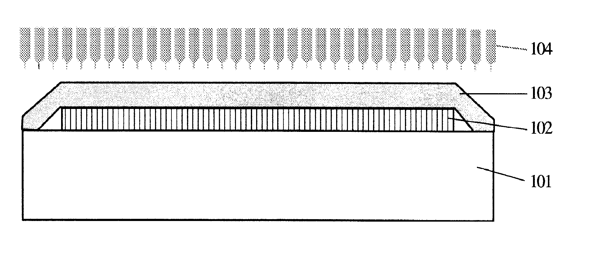
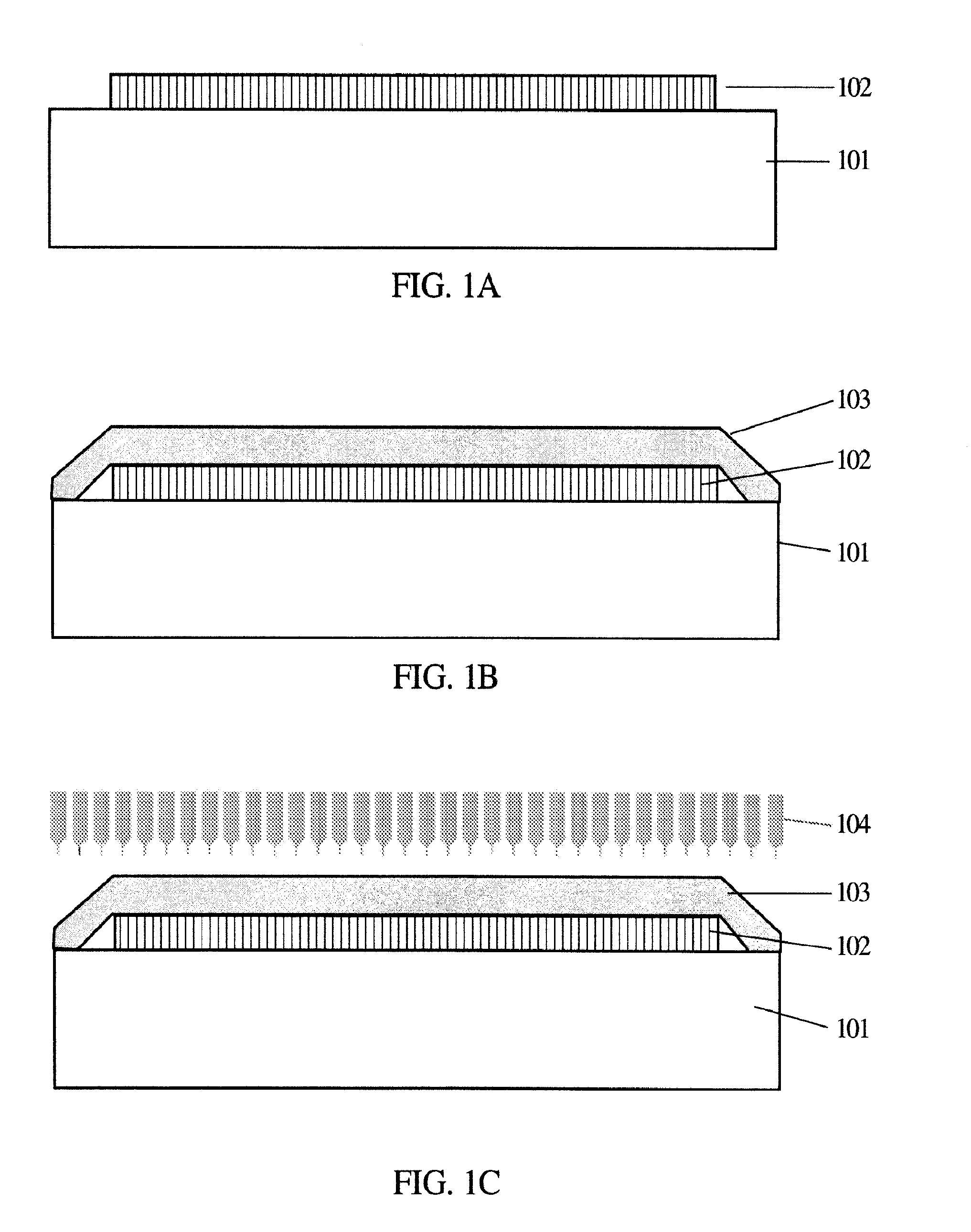
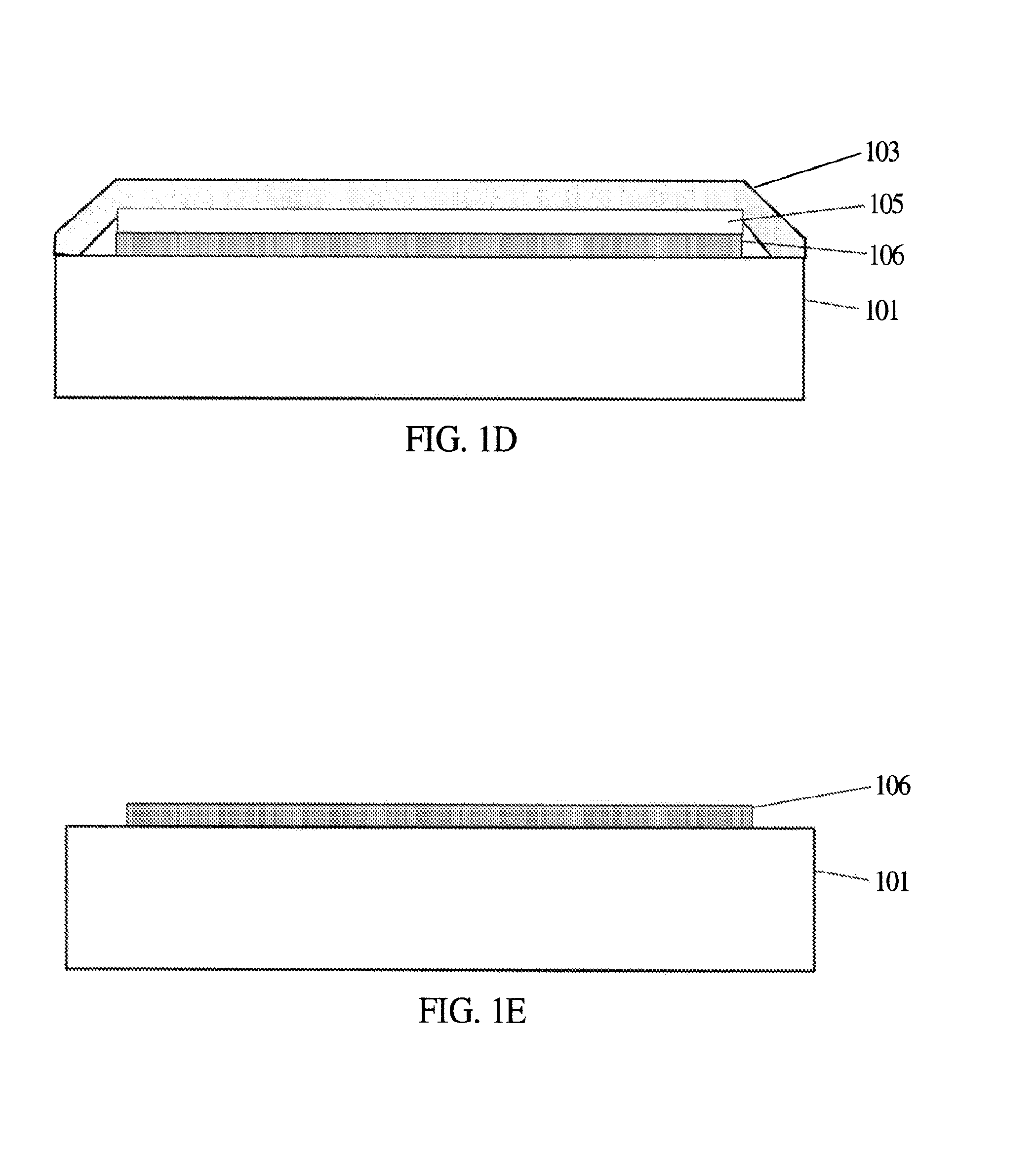
[0026]In order to maintain film density and conductivity while providing sufficient adhesion, there needs to be consideration for maintaining the adhesive promoter outside the surface coating film. Embodiments described herein implement placement of a cover film on top of a dried copper nanoparticle film. The cover layer acts to provide a thermal transfer buffer to decrease heat loss to the outside environment, inhibit a residue from remaining inside the resulting film, and confine any inter-particle motion in the film to the X,Y plane inhibiting ablation in a Z direction.

[0027]During a “flash lamp” curing parameter optimization study of dried copper ink film on a flexible substrate, a substrate was secured to a thick paper support with strips of translucent tape at the edges. It was noticed that after exposure to the flash lamp, the edges of the substrate under the tape yielded a copper film. When the tape was removed, a conductive copper film remained at those edges. Prompted by t...


PUM

PropertyMeasurementUnit
sizeaaaaaaaaaa
timeaaaaaaaaaa
conductiveaaaaaaaaaa

Abstract

Tape lamination on a dry copper ink film, followed by a flash lamp procedure, produces conductive films. The tape lamination increases the curing parameter window and reduces crack formation in the metallic film Tape lamination facilitates curing of a continuous copper film on temperature sensitive substrates, such as PET, at power levels that would usually crack blow off the copper film This lamination process also improves adhesion and uniformity of the cured film.

Description

[0001]This application claims priority to U.S. Provisional Patent Application Ser. No. 61 / 543,557, which is hereby incorporated by reference heroin.BACKGROUND AND SUMMARY[0002]Sintering copper ink or paste films applied to low melting point flexible films (e.g., PET, PEN), is problematic, since the substrate material would be thermally damaged at typical copper sintering temperatures. Photosintering (or photonic “flash lamp” sintering) can be used to create conductive films from metallic nanoparticles. Photosintering is a process whereby nanoparticles are exposed to a high-intensity light, the nanoparticles absorb the light and convert the energy to heat, and the particles begin to melt, assuming an energy threshold required to increase the temperature above their melting, point is achieved. Photosintering can be accomplished using broad band (such as produced by a Xe-arc discharge lamp or coherent light (such as produced by a laser) sources. The photosintering process is extremely ...

Claims


Application Information

Patent Timeline
Patent Type & Authority Applications(United States)
IPC IPC(8): H01B13/00
CPCH01B13/003H01B1/026H01B1/22H05K3/1283H05K2201/0145
Inventor FINK, RICHARD LEENOVAK, JAMES P.GINSBERG, VALERIE
Owner APPLIED NANOTECH HLDG
Why Eureka
Try Eureka