Semiconductor device

a semiconductor and device technology, applied in semiconductor devices, instruments, electrical apparatus, etc., can solve the problems of increased threshold voltage change, poor electrical characteristics of transistors, and defect formation at the side surface, so as to reduce oxygen vacancies, improve yield, and excellent electrical characteristics

Active Publication Date: 2014-11-20
SEMICON ENERGY LAB CO LTD
View PDF7 Cites 70 Cited by
  • Summary
  • Abstract
  • Description
  • Claims
  • Application Information

AI Technical Summary

Benefits of technology

[0019]When the first or second gate electrode faces a side surface of the oxide semiconductor film with the gate insulating film therebetween in the channel width direction of the transistor, formation of a parasitic channel at the side surface of the oxide semiconductor film and its vicinity is suppressed because of an electric field of the first or second gate electrode. As a result, drain current is drastically increased at the threshold voltage, so that the transistor has excellent electrical characteristics. Further, in the channel width direction of the transistor, the minimum distance between the side surface of the oxide semiconductor film and the second gate electrode is preferably greater than or equal to 0.5 μm and less than or equal to 1.5 μm. In that case, a short circuit between the oxide semiconductor film and the second gate electrode can be prevented, which can increase yield.
[0020]Further, when the gate insulating film, the first gate insulating film, or the second gate insulating film includes an oxide insulating film containing a higher proportion of oxygen than that of oxygen in the stoichiometric composition, oxygen contained in the gate insulating film, the first gate insulating film, or the second gate insulating film is transferred to the oxide semiconductor film, which can reduce oxygen vacancies in the oxide semiconductor film. As a result, the transistor has normally-off characteristics. Further, the amount of change in electrical characteristics, typically in threshold voltage, of the transistor due to passage of time or a stress test can be reduced.
[0021]According to one embodiment of the present invention, a semiconductor device which includes an oxide semiconductor and in which formation of a parasitic channel due to a gate BT stress is suppressed can be provided. Further, a semiconductor device including a transistor having excellent electrical characteristics can be provided.

Problems solved by technology

In a transistor including an oxide semiconductor film, a large number of defects in the oxide semiconductor film cause poor electrical characteristics of the transistor and cause an increase in the amount of change in threshold voltage due to passage of time or a stress test (e.g., a bias-temperature (BT) stress test).
Defects are formed at the side surface of the oxide semiconductor film because of damage due to processing for element isolation, and the side surface of the oxide semiconductor film is polluted by attachment of impurities, or the like.
The transistor having normally-on characteristics causes various problems in that malfunction is likely to be caused when a semiconductor device is in operation and that power consumption is increased when a semiconductor device is not in operation.
Further, there is a problem in that the amount of change in electrical characteristics, typically in threshold voltage, of the transistor is increased by passage of time or a stress test.

Method used


Image

  • Semiconductor device
  • Semiconductor device
  • Semiconductor device

Examples


embodiment 1

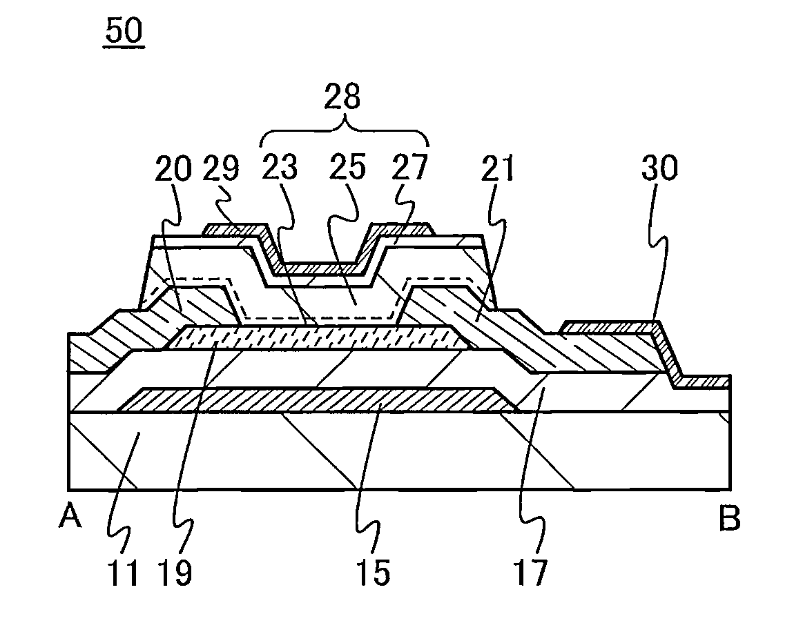
[0047]In this embodiment, a semiconductor device that is one embodiment of the present invention and a manufacturing method thereof are described with reference to drawings.

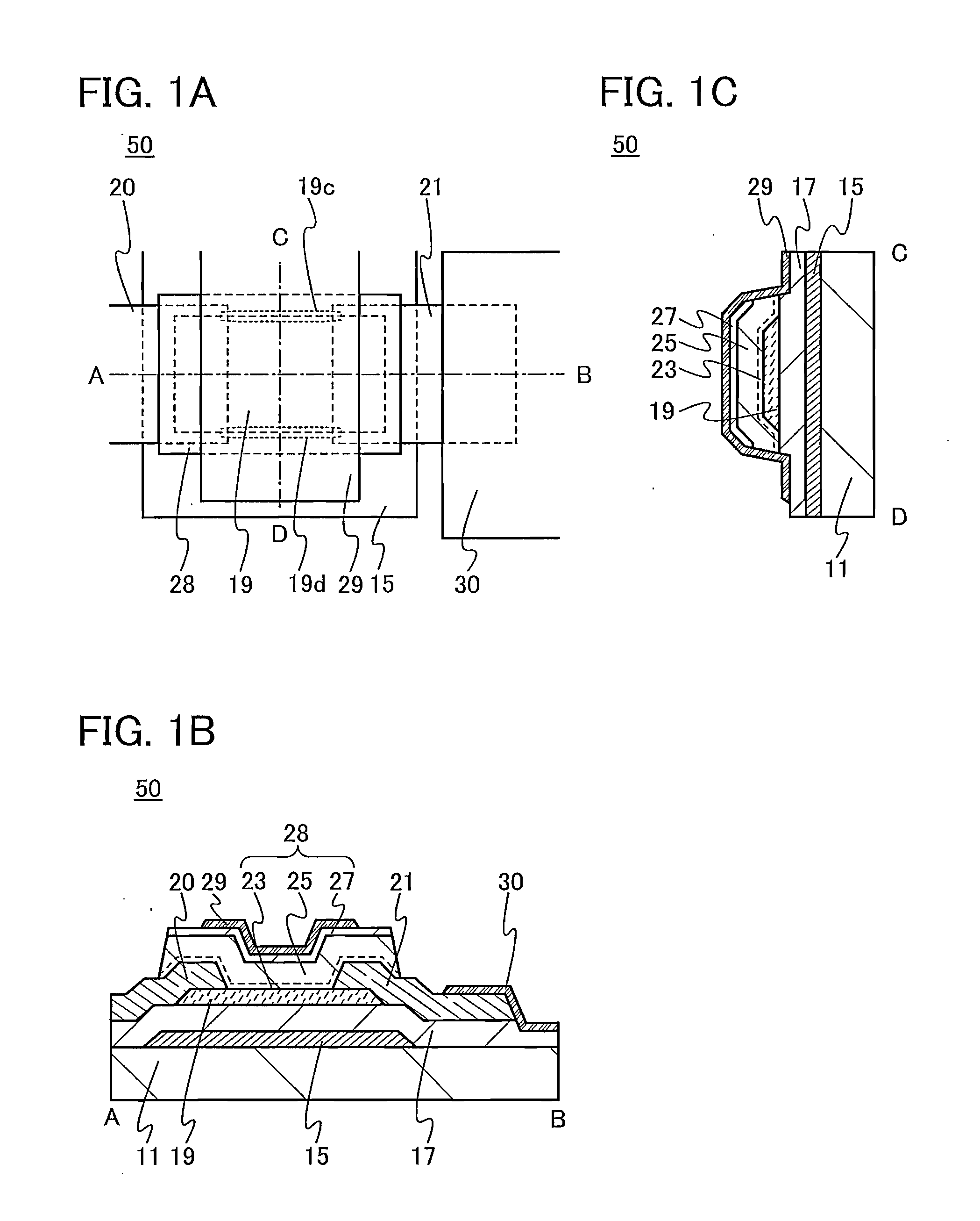
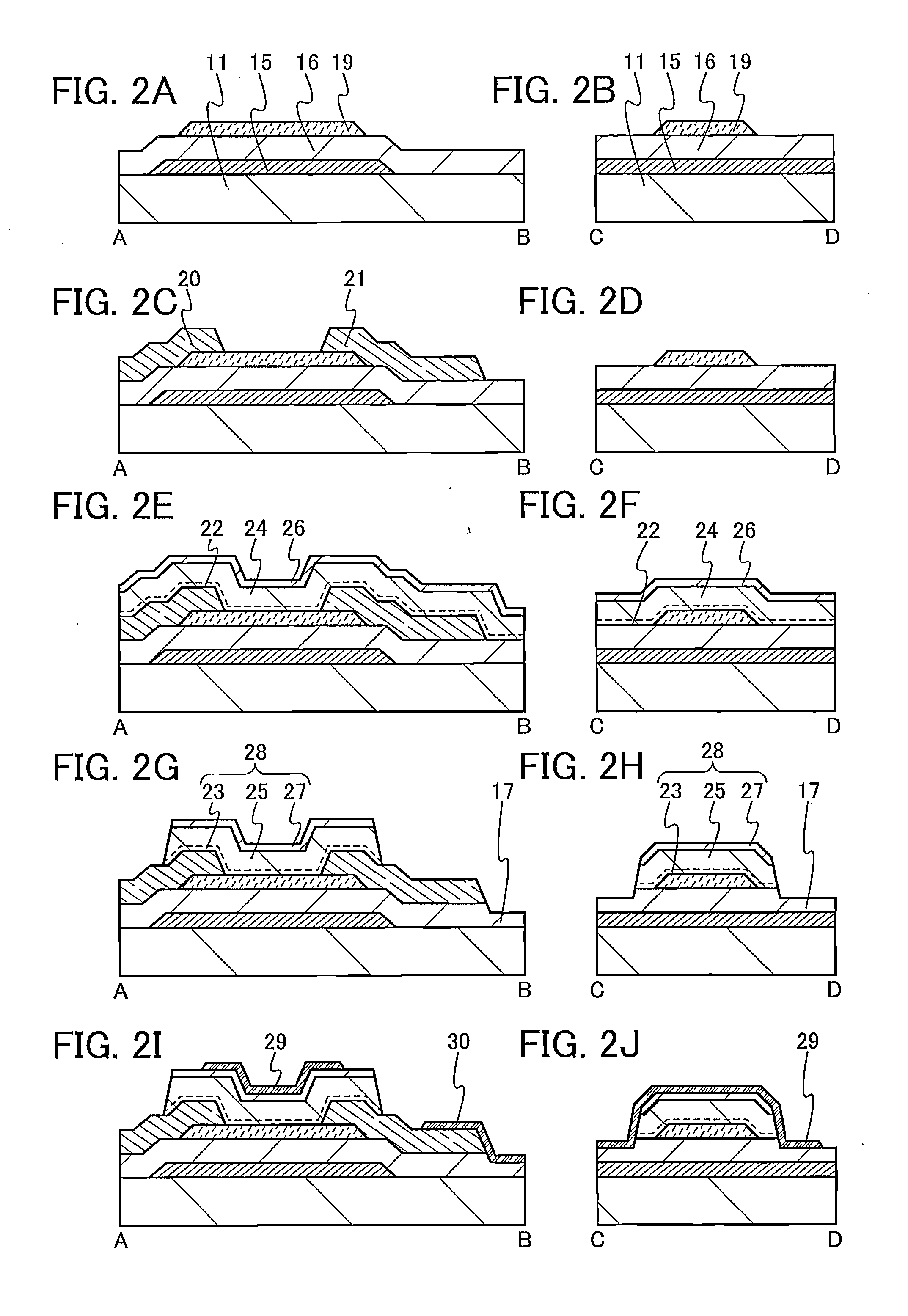
[0048]A top view and cross-sectional views of a transistor 50 included in a semiconductor device are illustrated in FIGS. 1A to 1C. The transistor 50 illustrated in FIGS. 1A to 1C is a channel-etched transistor. FIG. 1A is a top view of the transistor 50, FIG. 1B is a cross-sectional view taken along dashed-dotted line A-B in FIG. 1A, and FIG. 1C is a cross-sectional view taken along dashed-dotted line C-D in FIG. 1A. Note that in FIG. 1A, a substrate 11, a gate insulating film 17, an oxide insulating film 23, an oxide insulating film 25, a nitride insulating film 27, and the like are omitted for simplicity.

[0049]The transistor 50 illustrated in FIGS. 1B and 1C includes a gate electrode 15 over the substrate 11; the gate insulating film 17 over the substrate 11 and the gate electrode 15; an oxide semiconductor fi...

embodiment 2

[0163]In this embodiment, a semiconductor device and a manufacturing method thereof, which are different from those in Embodiment 1, are described with reference to drawings. This embodiment differs from Embodiment 1 in that a protective film is not isolated for each transistor.

[0164]A top view and cross-sectional views of a transistor 60 included in a semiconductor device are illustrated in FIGS. 5A to 5C. The transistor 60 illustrated in FIGS. 5A to 5C is a channel-etched transistor. FIG. 5A is a top view of the transistor 60, FIG. 5B is a cross-sectional view taken along dashed-dotted line A-B of FIG. 5A, and FIG. 5C is a cross-sectional view taken along dashed-dotted line C-D of FIG. 5A. Note that in FIG. 5A, the substrate 11, a gate insulating film 31, an oxide insulating film 33, an oxide insulating film 35, a nitride insulating film 37 and the like are omitted for simplicity.

[0165]The transistor 60 illustrated in FIGS. 5B and 5C includes the gate electrode 15 over the substra...

embodiment 3

[0190]In this embodiment, the electrical characteristics of the transistor having a dual-gate structure described in Embodiments 1 and 2 that includes gate electrodes connected to each other and having the same potential are described with reference to FIGS. 1A to 1C and FIG. 7A to FIG. 12C.

[0191]Note that here a driving method in which the gate electrodes 15 and 29 in FIG. 1A are electrically short-circuited and are supplied with a gate voltage is referred to as dual-gate driving. In other words, in dual-gate driving, the voltage of the gate electrode 15 is always equal to that of the gate electrode 29.

[0192]Here, the electrical characteristics of the transistor were evaluated. FIGS. 7A and 7B illustrate the structures of transistors used for the calculation. Note that device simulation software “Atlas” produced by Silvaco Inc. was used for the calculation.

[0193]A transistor having Structure 1 in FIG. 7A is a dual-gate transistor.

[0194]In the transistor having Structure 1, an insul...


PUM

PropertyMeasurementUnit
distanceaaaaaaaaaa
sizesaaaaaaaaaa
sizesaaaaaaaaaa

Abstract

A semiconductor device which includes an oxide semiconductor and in which formation of a parasitic channel due to a gate BT stress is suppressed is provided. Further, a semiconductor device including a transistor having excellent electrical characteristics is provided. The semiconductor device includes a transistor having a dual-gate structure in which an oxide semiconductor film is provided between a first gate electrode and a second gate electrode; gate insulating films are provided between the oxide semiconductor film and the first gate electrode and between the oxide semiconductor film and the second gate electrode; and in the channel width direction of the transistor, the first or second gate electrode faces a side surface of the oxide semiconductor film with the gate insulating film between the oxide semiconductor film and the first or second gate electrode.

Description

TECHNICAL FIELD[0001]The present invention relates to a semiconductor device having a transistor including an oxide semiconductor film and a method for manufacturing the semiconductor device.BACKGROUND ART[0002]Attention has been focused on a technique for forming a transistor using a semiconductor thin film formed over a substrate (also referred to as a thin film transistor (TFT)). Such a transistor is applied to a wide range of electronic devices such as an integrated circuit (IC) or an image display device (display device). A silicon-based semiconductor material is widely known as a material for a semiconductor thin film applicable to a transistor. As another material, an oxide semiconductor has been attracting attention.[0003]For example, a transistor including an oxide semiconductor containing indium (In), gallium (Ga), and zinc (Zn) as an active layer of the transistor has been disclosed (see Patent Document 1).[0004]Further, a technique of improving carrier mobility by formin...

Claims


Application Information

Patent Timeline
Patent Type & Authority Applications(United States)
IPC IPC(8): H01L27/12G02F1/1362
CPCG02F1/136277H01L27/1225G02F1/1368H01L29/7869H01L29/78696H01L29/78648G02F1/134309H01L27/1237H01L27/124
Inventor YAMAZAKI, SHUNPEIMIYAKE, HIROYUKIOKAZAKI, KENICHIHAYAKAWA, MASAHIKOMATSUDA, SHINPEI
Owner SEMICON ENERGY LAB CO LTD
Why Eureka
Try Eureka