Etch process for reducing directed self assembly pattern defectivity using direct current positioning

a direct current positioning and pattern technology, applied in photomechanical treatment, instruments, electrical equipment, etc., can solve problems such as inacceptable line edge roughness/line width roughness (ler/lwr), limitation of phase numbers, and conventional etching techniques that have produced pattern defectivity, etc., to reduce directed self-assembly pattern defectivity

Active Publication Date: 2014-12-18
TOKYO ELECTRON LTD
View PDF3 Cites 27 Cited by
  • Summary
  • Abstract
  • Description
  • Claims
  • Application Information

AI Technical Summary

Benefits of technology

[0009]A method for preparing a patterned directed self-assembly layer for reducing directed self-assembly pattern defectivity using direct current superpositioning is provided. A substrate having a block copolymer layer overlying an intermediate layer, said block copolymer layer comprising a first phase-separated polymer defining a first pattern and a second phase-separated polymer defining a second pattern in said block copolymer layer is provided. A first plasma etching process using plasma formed of a first process composition to remove said second phase-separated polymer w...

Problems solved by technology

When applied in a thin film, the geometric confinement may pose additional boundary conditions that may limit the numbers of phases.
However, when removing a polystyrene-b-poly(methyl methacrylate) (PMMA) from a p...

Method used


Image

  • Etch process for reducing directed self assembly pattern defectivity using direct current positioning
  • Etch process for reducing directed self assembly pattern defectivity using direct current positioning
  • Etch process for reducing directed self assembly pattern defectivity using direct current positioning

Examples


Embodiment Construction

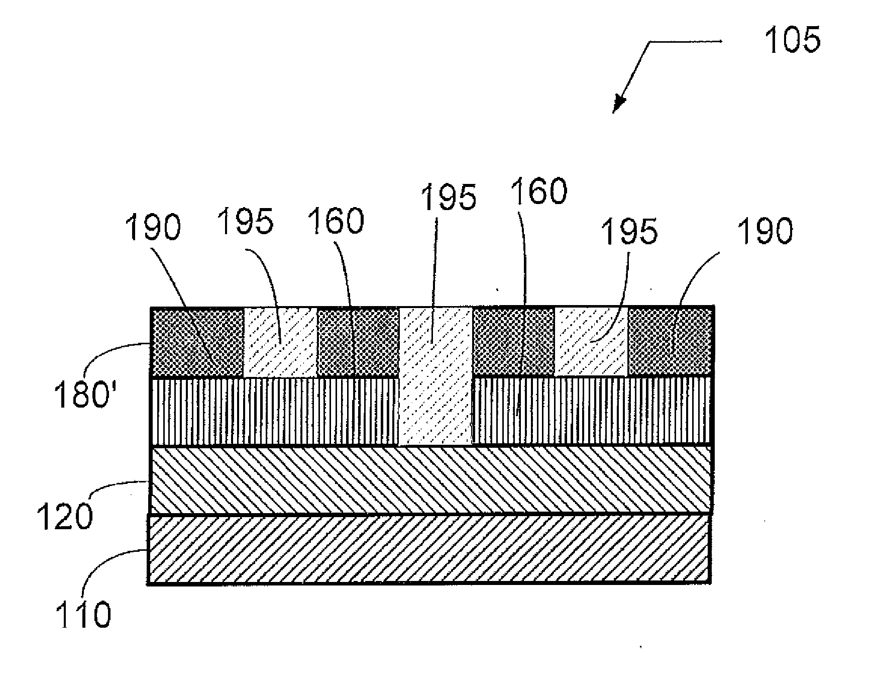
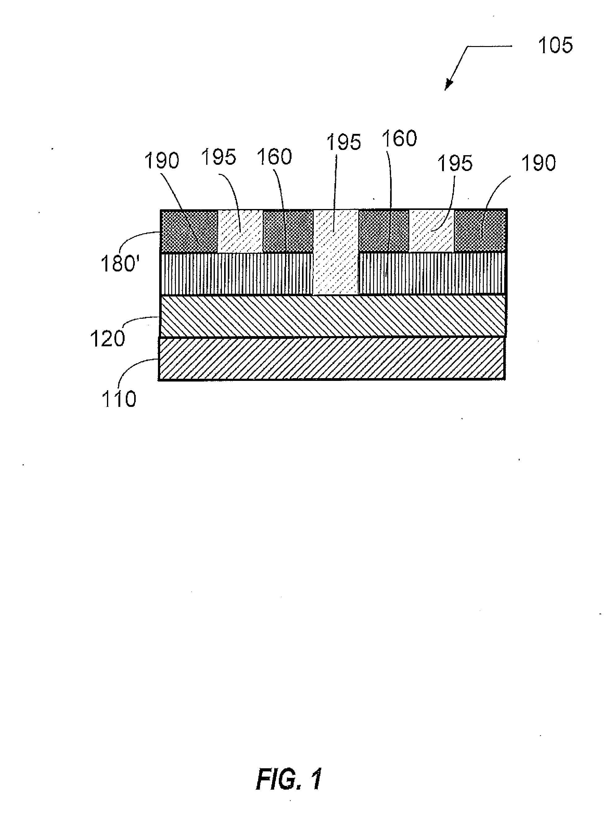
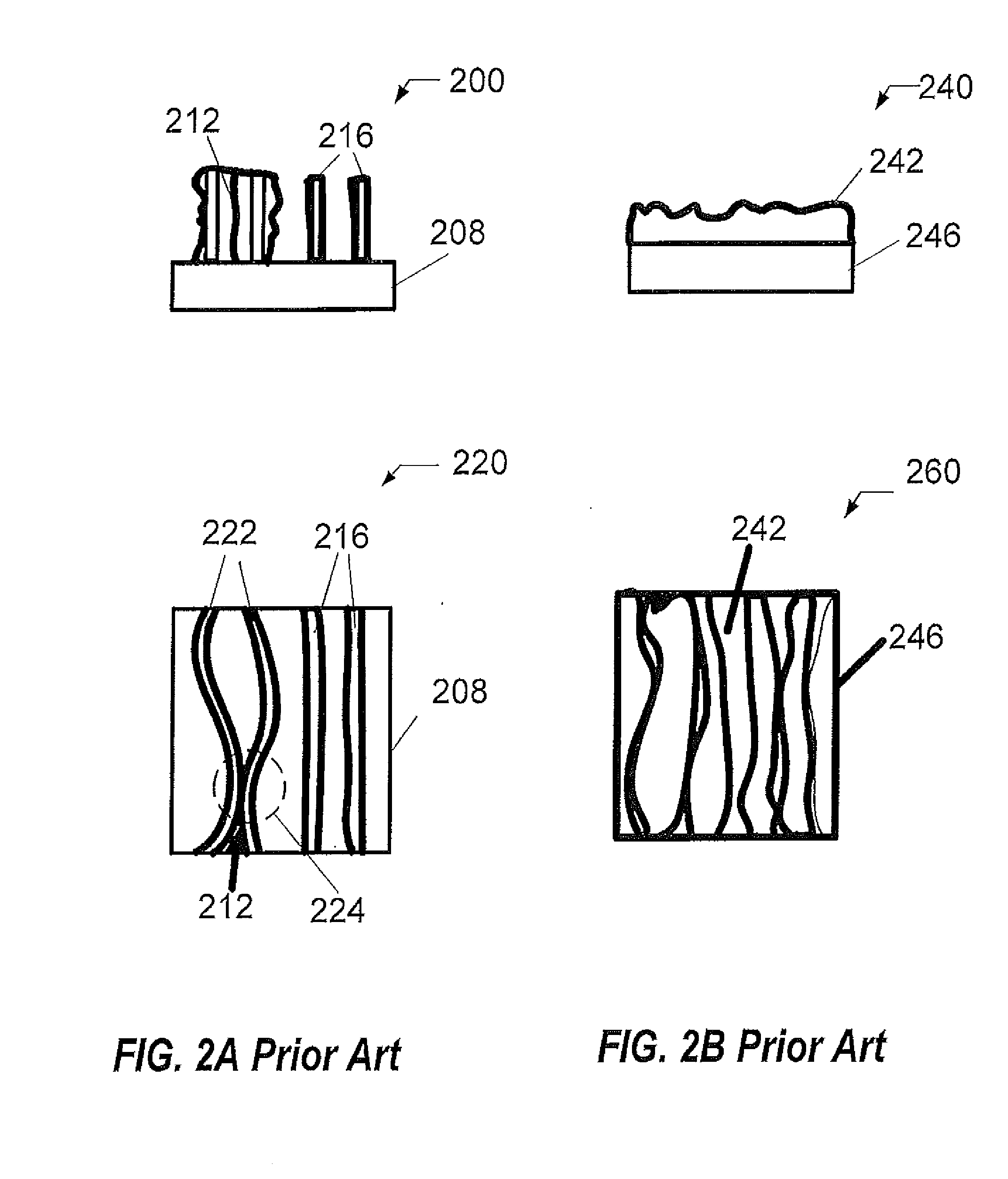
[0023]Materials and methods for forming a layered substrate comprising a self-assembled material are disclosed in various embodiments. However, one skilled in the relevant art will recognize that the various embodiments may be practiced without one or more of the specific details, or with other replacement and / or additional methods, materials, or components. In other instances, well-known structures, materials, or operations are not shown or described in detail to avoid obscuring aspects of various embodiments of the invention.

[0024]Similarly, for purposes of explanation, specific numbers, materials, and configurations are set forth in order to provide a thorough understanding of the invention. Nevertheless, the invention may be practiced without specific details. Furthermore, it is understood that the various embodiments shown in the figures are illustrative representations and are not necessarily drawn to scale. In referencing the figures, like numerals refer to like parts through...


PUM


Abstract

A method for preparing a patterned directed self-assembly layer for reducing directed self-assembly pattern defectivity using direct current superpositioning is provided. A substrate having a block copolymer layer overlying a first intermediate layer, said block copolymer layer comprising a first phase-separated polymer defining a first pattern and a second phase-separated polymer defining a second pattern in said block copolymer layer is provided. A first plasma etching process using plasma formed of a first process composition to remove said second phase-separated polymer while leaving behind said first pattern of said first phase-separated polymer is performed. A second plasma etching process to transfer said first pattern into said first intermediate layer using plasma formed of a second process composition is performed. In an embodiment, said first phase-separated polymer is exposed to an electron beam preceding, during, or following said first plasma etching process, or preceding or during said second plasma etching process.

Description

FIELD OF THE INVENTION[0001]This disclosure is related to methods for forming patterns in layered articles, and the layered articles formed therefrom; and more specifically, to reducing pattern collapse and other pattern defectivity in directed self-assembly applications using direct current superpositioning.BACKGROUND OF THE INVENTION[0002]The need to remain competitive in cost and performance in the production of semiconductor devices has caused a continuous increase in device density of integrated circuits. To accomplish higher integration and miniaturization in a semiconductor integrated circuit, miniaturization of a circuit pattern formed on a semiconductor wafer must also be accomplished.[0003]Photolithography is a standard technique used to manufacture semiconductor integrated circuitry by transferring geometric shapes and patterns on a mask to the surface of a semiconductor wafer. However, current state-of-the-art photolithography tools allow minimum feature sizes down to ab...

Claims


Application Information

Patent Timeline
IPC IPC(8): H01L21/311H01L21/263
CPCH01L21/263H01L21/31138H01L21/0337H01L21/67103H01L21/67109H01L21/67248B81C1/00031B81C2201/0149G03F7/0002
Inventor CHAKRAPANI, VIDHYAKO, AKITERUKUMAR, KAUSHIK
Owner TOKYO ELECTRON LTD
Why Eureka
Try Eureka