Integrated MEMS pressure sensor with mechanical electrical isolation

Inactive Publication Date: 2015-03-05
WINDTOP TECH CORP
View PDF0 Cites 40 Cited by
  • Summary
  • Abstract
  • Description
  • Claims
  • Application Information

AI Technical Summary

Benefits of technology

[0006]Another object of the present invention is to provide a MEMS

Problems solved by technology

The problem with the two-chip solutions using wire bonding is that the wire is basically an inductive antenna and can pickup high frequency noise whose har

Method used


Image

  • Integrated MEMS pressure sensor with mechanical electrical isolation
  • Integrated MEMS pressure sensor with mechanical electrical isolation
  • Integrated MEMS pressure sensor with mechanical electrical isolation

Examples


Embodiment Construction

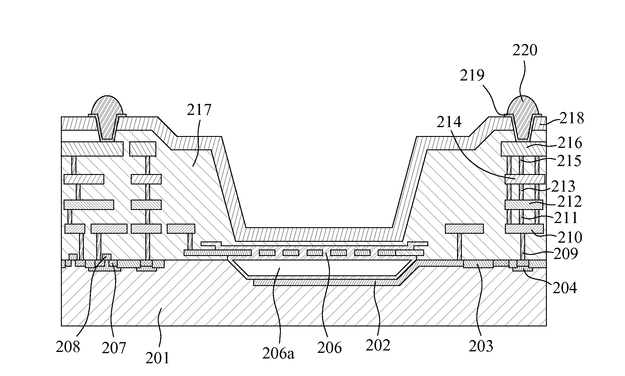
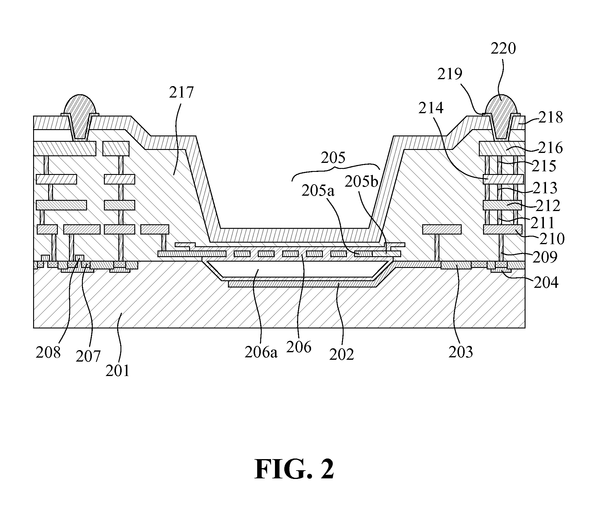
[0014]FIG. 2 shows a cross-sectional view of an exemplary embodiment of a MEMS device having a single chip structure fabricated to function as a MEMS pressure sensor according to the present invention. As shown in FIG. 2, the integrated MEMS pressure sensor of the present invention combines CMOS ASIC and MEMS and uses flip chip package technology to fabricate. From the bottom up, the structure of an integrated MEMS pressure sensor of the present invention includes a CMOS substrate layer 201, an N+ implant doped silicon layer 202, a field oxide (FOX) layer 203, a plurality of implant doped silicon areas 204 forming CMOS well, a two-tier polysilicon layer 205, further including an implant doped polysilicon layer 205a and a non-doped polysilicon layer 205b, a second non-doped polysilicon layer 206, a plurality of implant doped silicon areas 207 forming CMOS source / drain, a gate poly layer 208 made of polysilicon to form CMOS transistor gates, an oxide layer 217 embedded with an interco...


PUM

PropertyMeasurementUnit
Temperatureaaaaaaaaaa
Thicknessaaaaaaaaaa
Electrical conductivityaaaaaaaaaa

Abstract

An integrated MEMS pressure sensor is provided, including, a CMOS substrate layer, an N+ implant doped silicon layer, a field oxide (FOX) layer, a plurality of implant doped silicon areas forming CMOS wells, a two-tier polysilicon layer with selective ion implantation forming a membrane, including an implant doped polysilicon layer and a non-doped polysilicon layer, a second non-doped polysilicon layer, a plurality of implant doped silicon areas forming CMOS source/drain, a gate poly layer made of polysilicon forming CMOS transistor gates, said CMOS wells, CMOS transistor sources/drains and CMOS gates forming CMOS transistors, an oxide layer embedded with an interconnect contact layer, a plurality of metal layers interleaved with a plurality of via hole layers, a Nitride deposition layer, an under bump metal (UBM) layer and a plurality of solder spheres. N+ implant doped silicon layer and implant doped/un-doped composition polysilicon layer forming a sealed vacuum chamber.

Description

FIELD OF THE INVENTION[0001]The present invention generally relates to an integrated MEMS device, and more specifically to an integrated MEMS device built with CMOS process, Flip Chip Bumping package or WLP (Wafer Level Package) technology with mechanical / electrical isolation capability.BACKGROUND OF THE INVENTION[0002]MEMS devices have long been attracting attentions due to a wide range of portable applications. For example, MEMS pressure sensor as altimeter has recently gained attraction due to the use of portable devices such as smart phones. MEMS pressure sensors can be made with resistor type or capacitive type. However, most of the MEMS pressure sensors were made with separate MEMS sensors and ASIC circuits with the final products assembled by wire bonding on top of a PCB substrate.[0003]FIG. 1 shows a schematic view of a conventional structure of a MEMS pressure sensor with two-chip structure. As shown in FIG. 1, a two-chip structure of a MEMS pressure sensor includes a print...

Claims


Application Information

Patent Timeline
IPC IPC(8): B81B7/00B81B3/00B81C1/00
CPCB81B7/0006B81B3/0021B81C1/00134B81B2201/0264B81B2207/015B81C1/00246B81C2203/0742G01L9/0045G01L9/0073
Inventor CHEN, KUN-LUNG
Owner WINDTOP TECH CORP
Why Eureka
Try Eureka