

Piezoelectric element
a technology of piezoelectric elements and piezoelectric plates, applied in piezoelectric/electrostrictive/magnetostrictive devices, piezoelectric/electrostriction/magnetostriction machines, electrical apparatus, etc., can solve problems such as reliability and productivity, and achieve the effects of improving piezoelectric properties, easy formation, and high self-orientation
- Summary
- Abstract
- Description
- Claims
- Application Information
AI Technical Summary
Benefits of technology
Problems solved by technology
Method used
Image

Examples
example 1
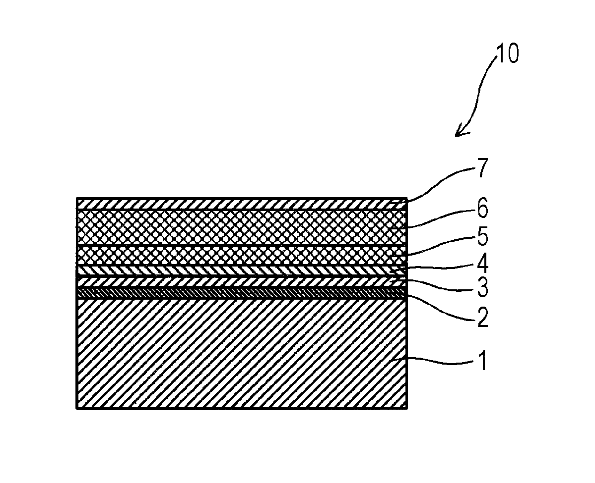
[0057]First, as illustrated in FIG. 6A, a thermal oxide film 2 made of SiO2 with a thickness of about 100 nm was formed on a substrate 1 made of a single-crystal Si wafer with a thickness of about 400 μm. Note that the substrate 1 may be a standard substrate having a thickness of 300 to 725 pm and a diameter of 3 to 8 inches. The thermal oxide film 2 can be formed by using a heating furnace for wet oxidation and exposing the substrate 1 to a high temperature of about 1000 to 1200° C. in an oxygen atmosphere.
[0058]Subsequently, as illustrated in FIG. 6B, an adhesion layer 3 made of Ti with a thickness of about 10 nm and a lower electrode 4 made of Pt with a thickness of about 150 nm were formed in this order on the thermal oxide film 2 by sputtering. In this process, the Ti sputtering conditions were Ar flow rate: 20 sccm, pressure: 0.8 Pa, and RF power applied to target: 80 W, and the Pt sputtering conditions were Ar flow rate: 20 sccm, pressure: 0.5 Pa, RF power applied to target: ...
example 2
[0063]In Example 2, lead lanthanum zirconate titanate (PLZT) was used for the piezoelectric thin film 6 instead of PZT. Other processes are the same as those in Example 1. Specifically, PLZT to be the piezoelectric thin film 6 was formed by sputtering on the buffer layer 5 made of PLT. In this process, the PLZT sputtering conditions were Ar flow rate: 25 sccm, O2 flow rate: 0.8 sccm, pressure: 0.4 Pa, substrate temperature: 500° C., and RF power applied to target: 400 W. As a result, a PLZT film of (Pb1-xLax) (ZryTi1-y)1-x / 4O3 (x=7.5, y=0.6) was formed with a thickness of 4 pm.
[0064]FIG. 7 is a graph illustrating a result of carrying out 2θ / θ measurement of x-ray diffraction on the PLZT film formed by sputtering on PLT in the (100) orientation. E+n of the intensity (relative value) of the vertical axis in FIG. 7 represents x1010. FIG. 7 shows that, when a PLZT film is formed to be the piezoelectric thin film 6, the PLZT film is also in the form of perovskite crystals mainly oriented...
PUM
| Property | Measurement | Unit |
|---|---|---|
| grain size | aaaaa | aaaaa |
| grain size | aaaaa | aaaaa |
| grain size | aaaaa | aaaaa |
Abstract
Description
Claims
Application Information