Solder bump, method for forming a solder bump, substrate provided with solder bump, and method for manufacturing substrate

a technology of solder bump and solder bump, which is applied in the direction of auxillary welding devices, non-printed masks, and semiconductor/solid-state device details. it can solve the problems of low productivity and the problem of copper corrosion still unsolved, and achieve the effect of suppressing copper corrosion occurring in conventional soldering, high dimensional precision, and easy formation

Inactive Publication Date: 2015-04-30
TANIGUROGUMI CORP
View PDF18 Cites 4 Cited by
  • Summary
  • Abstract
  • Description
  • Claims
  • Application Information

AI Technical Summary

Benefits of technology

[0018]The solder bump forming method according to the present invention allows for the formation of a Cu—Ni—Sn intermetallic compound layer obtained by alloying of copper of the copper electrode and nickel included in the molten solder on a surface of the copper electrode. Thus, the intermetallic compound layer serves as a barrier layer against copper corrosion, and the barrier layer can prevent copper corrosion of the copper electrode, thereby allowing for the prevention of defects and disappearance of the copper electrode due to copper corrosion. As a result, reliability can be ensured in the copper electrode such as a copper land of the mounting substrate. Thus, when electronic components are soldered to a mounting substrate, copper corrosion occurring in conventional soldering can be suppressed. In addition, the present invention allows solder bumps having a desired constant thickness to be easily formed with high dimensional precision on a mounting substrate with a minute copper electrode. Thus, such a high-cost step as in the conventional art is unnecessary, thus allowing for increase in reliability and yield of joint portions at which electronic components are solder-bonded to the solder bumps. This is advantageous in terms of manufacturing a low-cost mounting substrate.
[0019]The mounting substrate manufacturing method according to the present invention can ensure reliability of a copper electrode such as a copper land of a mounting substrate and can suppress copper corrosion occurring in conventional soldering when electronic component are soldered to a mounting substrate. In addition, the manufacturing method allows solder bumps having a desired constant thickness to be easily formed with high dimensional precision on a mounting substrate with a minute copper electrode thereon. As a result, such a high-cost step as in the conventional art is unnecessary, thus allowing for increase in reliability and yield of joint portions at which electronic components are solder-bonded to the solder bumps, so that a low-cost mounting substrate can be manufactured.
[0020]FIG. 1 is a schematic perspective view depicting a substrate and a mask used in a solder bump forming method according to the present invention.
[0021]FIG. 2 are step diagrams (1) depicting one example of the solder bump forming method according to the invention.
[0022]FIG. 3 are step diagrams (2) depicting the one example of the solder bump forming method according to the invention.
[0023]FIG. 4 are a part of step diagrams depicting another example of the solder bump forming method according to the invention.

Problems solved by technology

However, the method of Patent Document 2 has a problem in that it is a method for forming solder bumps having different heights by squeegeeing the supplied solder paste with a squeegee jig, thus leading to low productivity.
Additionally, the dipping method described above is problematic in that the problem of copper corrosion still remains unsolved.

Method used


Image

  • Solder bump, method for forming a solder bump, substrate provided with solder bump, and method for manufacturing substrate
  • Solder bump, method for forming a solder bump, substrate provided with solder bump, and method for manufacturing substrate
  • Solder bump, method for forming a solder bump, substrate provided with solder bump, and method for manufacturing substrate

Examples


example 1

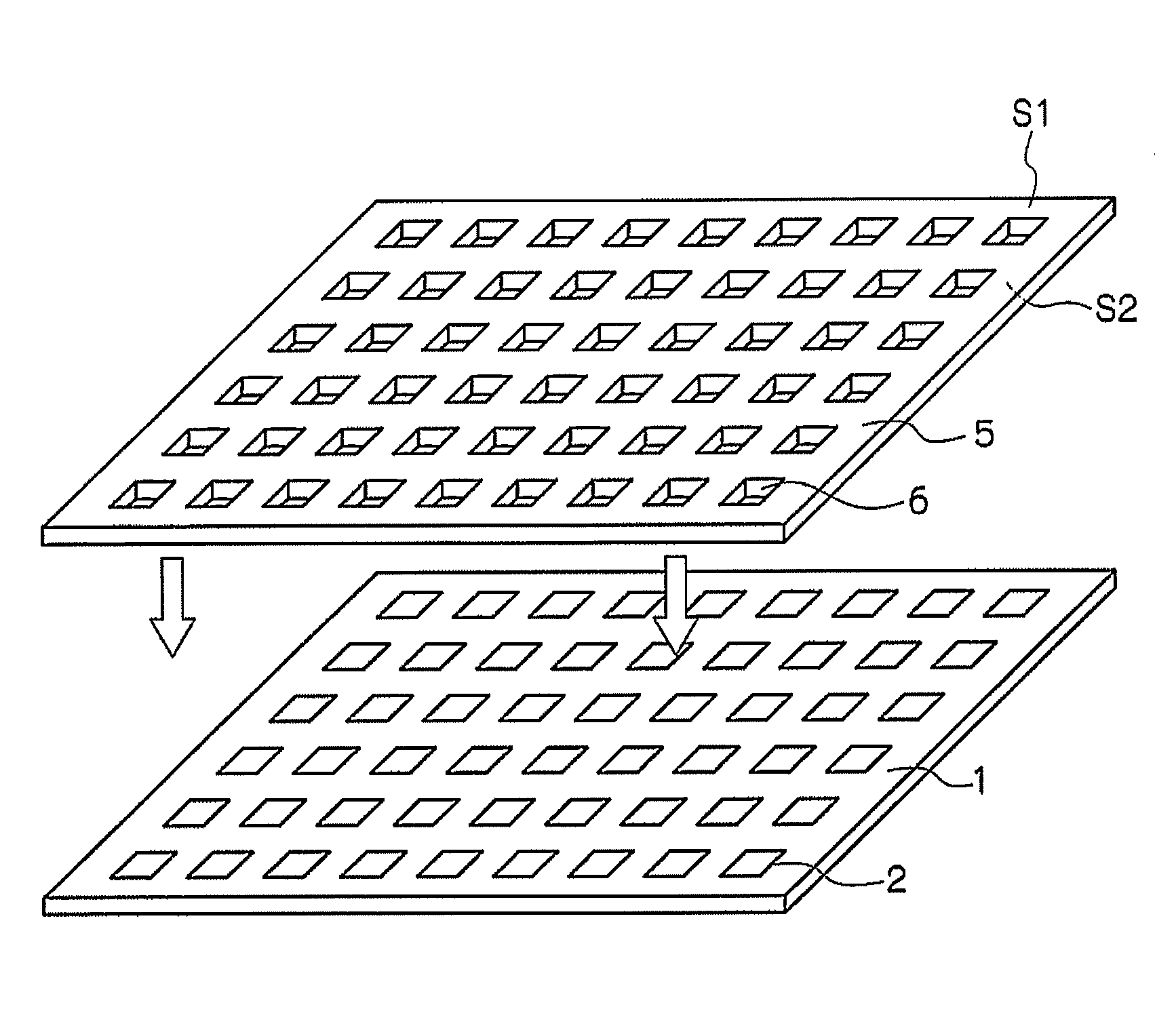
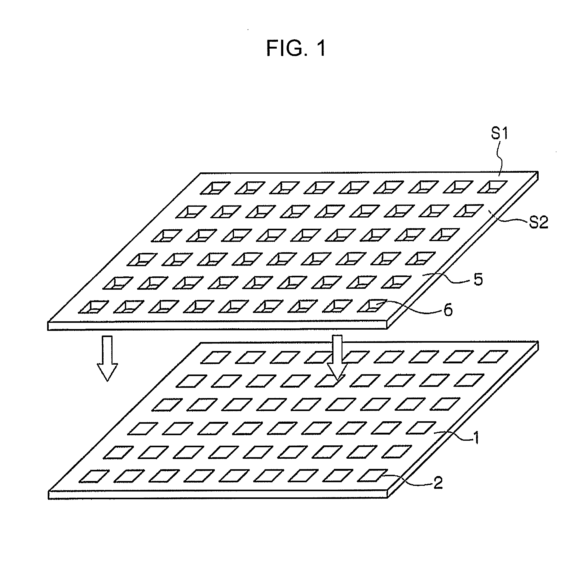
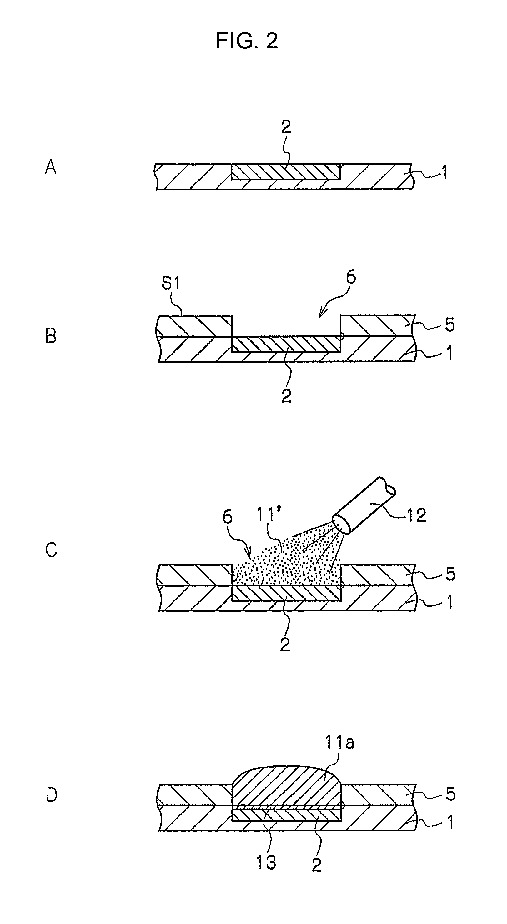
[0082]As one example, there was prepared substrate 1 having a copper wiring pattern having a width of, for example, 200 μm and a thickness of, for example, 10 μm formed thereon. On the substrate 1, there were exposed only joint portions of the copper wiring pattern that were to be portions for mounting electronic components and had a width of, for example, 200 μm and a length of, for example, 50 μm, whereas the other portions of copper electrode 2 were covered with an insulation layer. There was prepared mask 5 provided with opening portions 6 used for forming solder bumps 11 at such joint portions. Positions of the joint portions where copper electrode 2 was exposed on substrate 1 were matched with positions of the opening portions 6 of mask 5 to superimpose with each other. Then, using a quinary lead-free solder consisting of Ni: 0.05% by mass, Ge: 0.005% by mass, Ag: 3% by mass, Cu: 0.5% by mass, and Sn for the rest, the solder was heated to 250° C. to obtain molten solder 11a, a...

example 2

[0085]Solder bumps 11 according to Example 2 were formed in the same manner as in Example 1 except for using a quinary lead-free solder consisting of, as solder materials, Ni: 0.03% by mass, Ge: 0.005% by mass, Ag: 3% by mass, Cu: 0.5% by mass, and Sn for the rest. Similarly to Example 1, scanning electron micrographs of a section of obtained solder bump 11 were taken and indicated that Cu—Ni—Sn intermetallic compound layer 13a was formed with a thickness of 1 μm, although unevenness was slightly observed.

example 3

[0086]Solder bumps 11 according to Example 3 were formed in the same manner as in Example 1 except for using a quinary lead-free solder consisting of, as solder materials, Ni: 0.07% by mass, Ge: 0.005% by mass, Ag: 3% by mass, Cu: 0.5% by mass, and Sn for the rest. Similarly to Example 1, scanning electron micrographs of a section of obtained solder bump 11 were taken and indicated that Cu—Ni—Sn intermetallic compound layer 13a was formed uniformly with a thickness of 2 μm.


PUM

PropertyMeasurementUnit
widthaaaaaaaaaa
widthaaaaaaaaaa
widthaaaaaaaaaa

Abstract

Provided is a solder bump forming method capable of forming solder bumps having a desired constant thickness, without any failure such as copper corrosion, on a mounting board such as a printed circuit board having fine copper electrodes. The solder bump forming method includes: a process in which a prepared mask (5) is placed on a prepared substrate (1) and then a molten solder jet is blown to fill an opening of the mask (5) with molten solder (11a) until the molten solder (11a) exceeds the thickness of the mask (5); a process of removing a part of the molten solder (11a) that exceeds the thickness of the mask (5) to form a solder bump (11) having a predetermined thickness; and a process of removing the mask (5). The molten solder (11a) is molten lead-free solder that includes tin as a main ingredient and at least nickel as a sub ingredient, and further includes one or more other ingredients such as silver, copper, and germanium. The part of the molten solder (11a) that exceeds the thickness of the mask (5) is removed by using a blade or an air cutter or by spraying a solution (18) that includes organic fatty acid having 12 to 20 carbon atoms.

Description

FIELD OF THE INVENTION[0001]The present invention relates to a solder bump, a method for forming the solder bump, a substrate provided with the solder bump, and a method for manufacturing the substrate. More particularly, the invention relates to a solder bump having a constant thickness capable of preventing corrosion of copper forming a copper electrode on the copper electrode of a substrate such as a printed circuit board, a wafer, or a flexible substrate, a method for forming the solder bump, a substrate provided with the solder bump, and a method for manufacturing the substrate.BACKGROUND ART[0002]Recent years have seen increasing improvement in wiring density and mounting density on substrates such as printed circuit boards, wafers, and flexible substrates (which may be hereinafter referred to as “mounting substrates”). Solder bumps used for soldering electronic components on a mounting substrate are required to be minute and uniform in shape, size, and the like. As a solder b...

Claims


Application Information

Patent Timeline
Patent Type & Authority Applications(United States)
IPC IPC(8): B23K37/06H05K13/04
CPCH05K13/0465B23K37/06H01L21/4853H01L23/49811H01L24/05H01L24/11H01L24/13H01L2224/11849H01L2224/13118H01L2224/1312H01L2224/13139H01L2224/13111H01L2224/13113H01L2224/131H01L2224/1181H01L2224/11821H01L2224/11472H01L2224/11312H01L2224/05647H01L2224/05571H01L2224/05147H01L2224/05026H01L2224/0401H01L2224/16503H01L2224/13155H01L2224/94H01L2924/00014H01L2924/00012H01L2924/01028H01L2924/0105H01L2924/01047H01L2924/01029H01L2924/014H01L2924/0132H01L2224/11H01L2224/05552H05K3/282H05K3/3468H05K2203/0557H05K2203/0746H05K2203/1344
Inventor TANIGURO, KATSUMORI
Owner TANIGUROGUMI CORP
Why Eureka
Try Eureka