

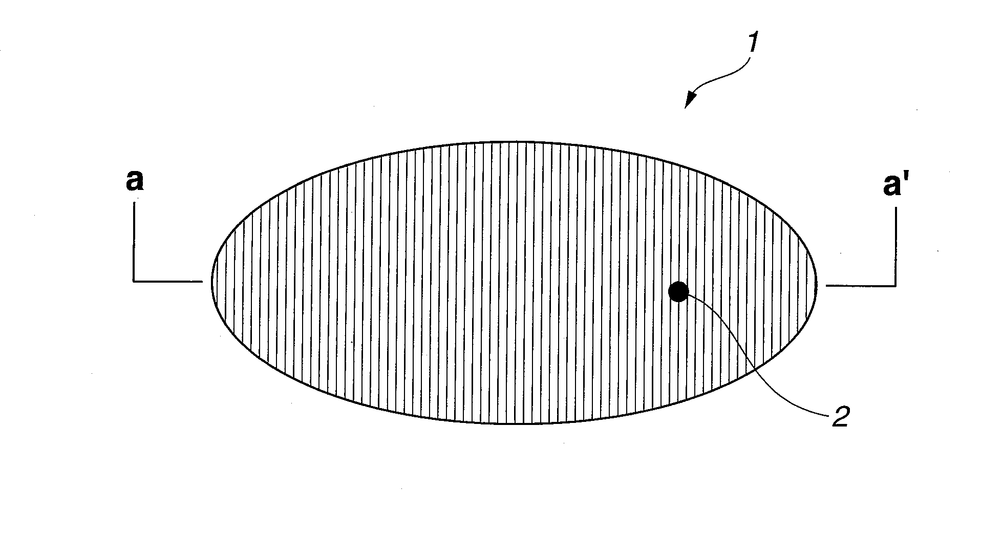
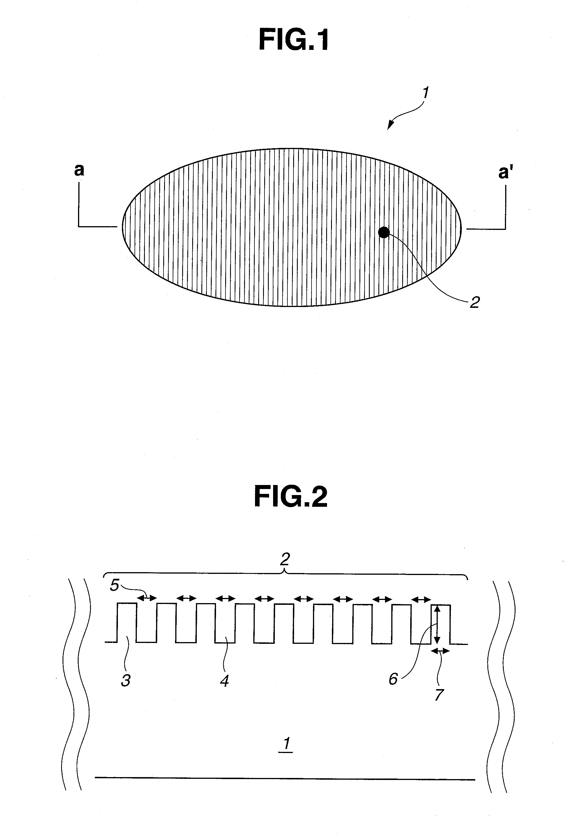
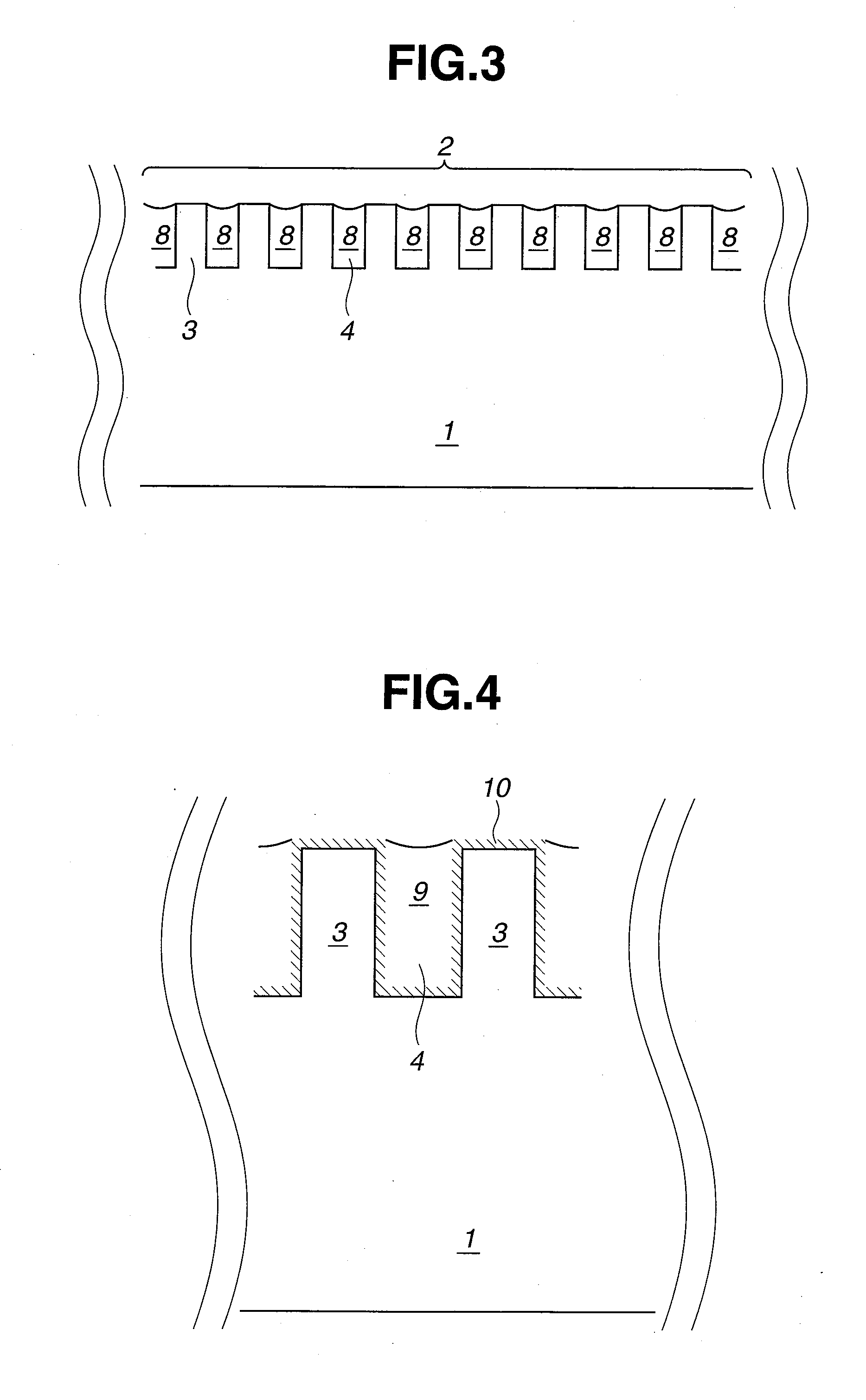
Water-Repellent Protective Film, and Chemical Solution for Forming Protective Film
a technology of water-repellent protective film and liquid chemical, which is applied in the direction of fluorine-based surface-active compounds, detergent compounding agents, other chemical processes, etc., can solve the problems of pattern collapse and its collapse, and achieve excellent water repellency, prevent pattern collapse, and reduce throughput
- Summary
- Abstract
- Description
- Claims
- Application Information
AI Technical Summary
Benefits of technology
Problems solved by technology
Method used
Image

Examples
example 1
(I-1) Preparation of Liquid Chemical for Forming Protective Film
[0140]A mixture of: 0.1 g of perfluorohexylethylphosphonic acid [C6F13C2H4P(O)(OH)2] that serves as a water-repellent protective film forming agent; and 0.2 g of isopropyl alcohol (hereinafter, referred to as “iPA”) was stirred at 25° C. to dissolve it. The thus obtained solution was mixed with 99.8 g of a solvent obtained by combining diethylene glycol monoethyl ether acetate (hereinafter, referred to as “DGEEA”) and water at a mass ratio of 94.8:5, with which the water-repellent protective film forming agent was dissolved within 1 minute and a uniform, clear, colorless solution was obtained. The solution was stirred for an additional 1 hour, thereby obtaining a liquid chemical for forming a protective film which liquid chemical had the concentration of the protective film forming agent (hereinafter referred to as “a protective film forming agent concentration”) of 0.1 mass % relative to the total amount of the liquid ...
examples 2 to 24
[0146]Upon modifying the conditions employed in Example 1 (as to the protective film forming agent, the protective film forming agent concentration, the solvent for the liquid chemical for forming a protective film, the order of producing the liquid chemical for forming a protective film (a first solvent and a second solvent), the temperature during the protective film-forming step, and the cleaning liquid B used in the subsequent cleaning step), a surface treatment was conducted on wafers, followed by evaluation of these. The results are shown in Table 1.
[0147]Incidentally, in Table, “C8H17P(O)(OH)2” means octylphosphonic acid, “PGME” means propylene glycol monomethyl ether, “DPGMEA” means dipropylene glycol monomethyl ether acetate, and “PGMEA” means propylene glycol monomethyl ether acetate.
example 25
(II-1) Preparation of Liquid Chemical for Forming Protective Film
[0148]A mixture of: 0.1 g of perfluorohexylethylphosphonic acid [C6F13C2H4P(O)(OH)2] that serves as a water-repellent protective film forming agent; and 0.2 g of iPA was stirred at 25° C. to dissolve it. The thus obtained solution was mixed with 99.8 g of a solvent obtained by combining DGEEA and water at a mass ratio of 94.8:5, with which the water-repellent protective film forming agent was dissolved within 1 minute and a uniform, clear, colorless solution was obtained. The solution was stirred for an additional 1 hour, thereby obtaining a liquid chemical for forming a protective film which liquid chemical had the protective film forming agent concentration of 0.1 mass %. Additionally, the appearance of the liquid chemical was visually observed, after cooling the liquid chemical to 0° C. or −30° C. for 24 hours and then bringing it back to room temperature (25° C.). As a result, the liquid chemical kept a condition o...
PUM
| Property | Measurement | Unit |
|---|---|---|
| temperature | aaaaa | aaaaa |
| aspect ratio | aaaaa | aaaaa |
| concentration | aaaaa | aaaaa |
Abstract
Description
Claims
Application Information