Deposition of heteroatom-doped carbon films

a carbon film and heteroatom technology, applied in the direction of instruments, coatings, transportation and packaging, etc., can solve the problems of increasing compressive stress, insufficient hardmasks for developing next-generation nand and dram devices, and difficult fabrication of further devices, etc., to achieve low compressive stress, ease compressive stress, and high etch selectivity and density

Active Publication Date: 2015-07-23
APPLIED MATERIALS INC
View PDF2 Cites 3 Cited by
  • Summary
  • Abstract
  • Description
  • Claims
  • Application Information

AI Technical Summary

Benefits of technology

[0011]Heteroatom-containing carbon-containing hardmasks have a high etch selectivity and density and a low compressive stress. Doping the carbon-containing hardmask with a heteroatom eases compressive stress while increasing hardmask density. Doping the carbon-containing hardmask with sulfur and / or phosphorous increases etch selectivity by making the hardmask less reactive to active species commonly used in etching processes, such as F−, Cl−, and Br−.

Problems solved by technology

Wafer bow can make further device fabrication difficult.
Current hardmasks are insufficient for developing next generation NAND and DRAM devices.
However, attempts at increasing etch selectivity have resulted in an increase in compressive stress, and attempts at decreasing compressive stress have resulted in a decrease in etch selectivity.

Method used


Image

  • Deposition of heteroatom-doped carbon films
  • Deposition of heteroatom-doped carbon films
  • Deposition of heteroatom-doped carbon films

Examples


Embodiment Construction

[0015]The descriptions of the various embodiments disclosed herein are presented for illustrative purposes and are not intended to be exhaustive. Many modifications and variations will be apparent to those of ordinary skill in the art without departing from the scope and spirit of the described embodiments. The terminology used herein was chosen to best explain the principles of the embodiments, the practical applications or technical improvements over technologies found in the marketplace, or to enable others of ordinary skill in the art to understand the embodiments disclosed herein.

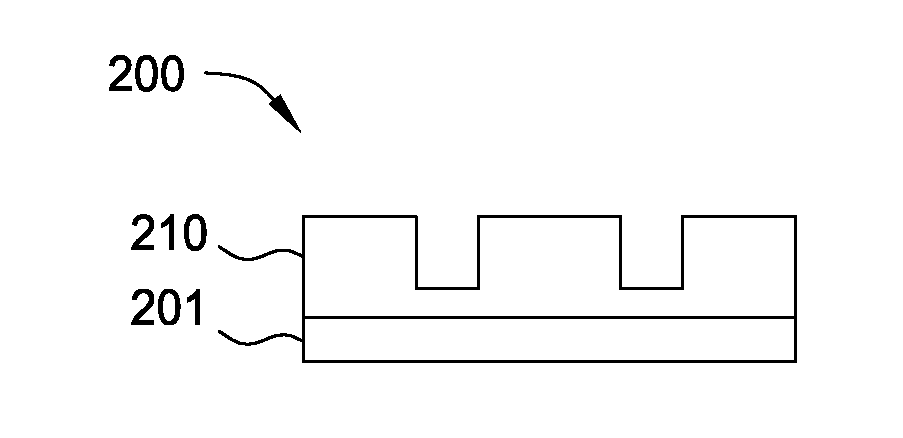
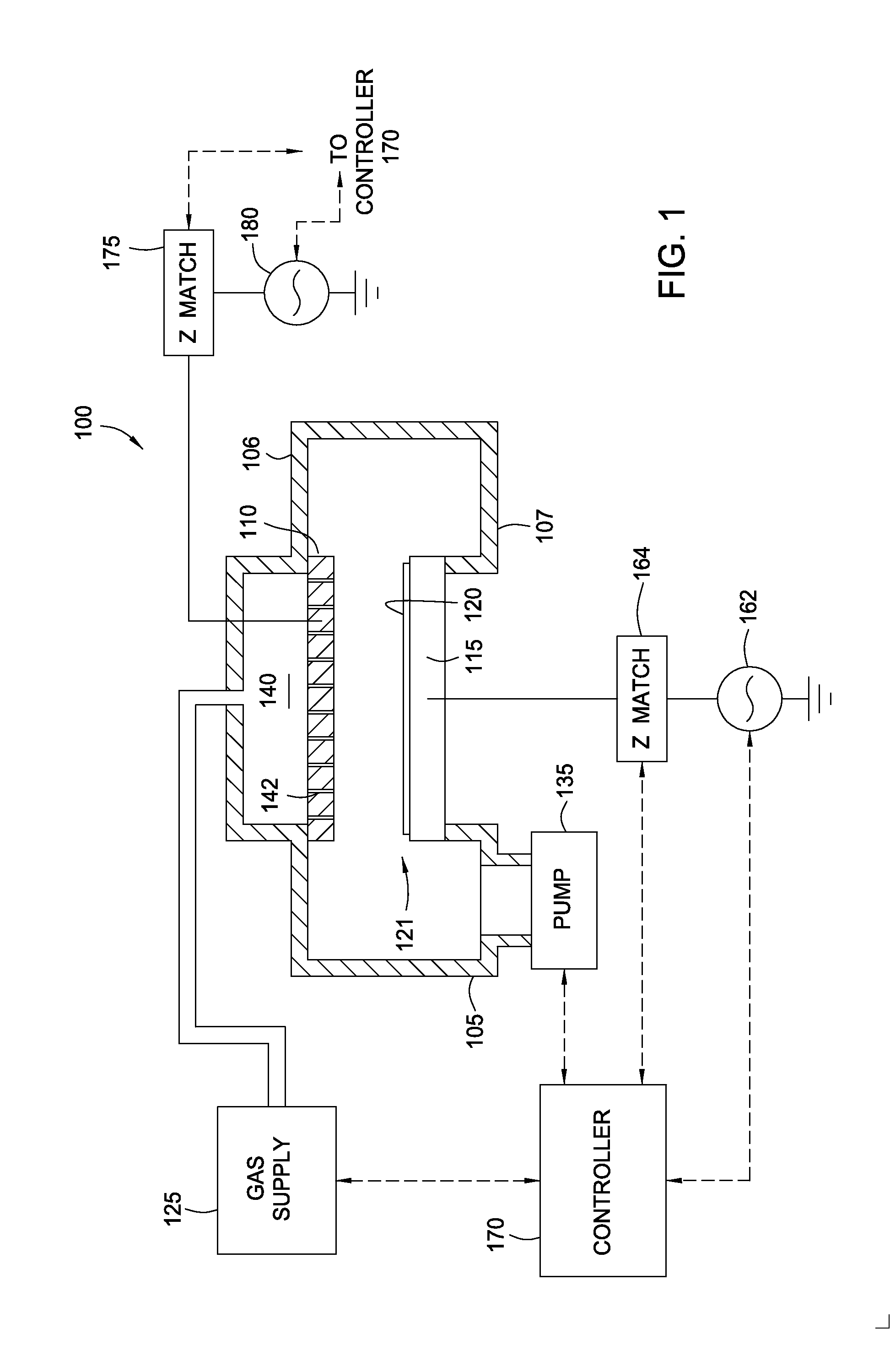
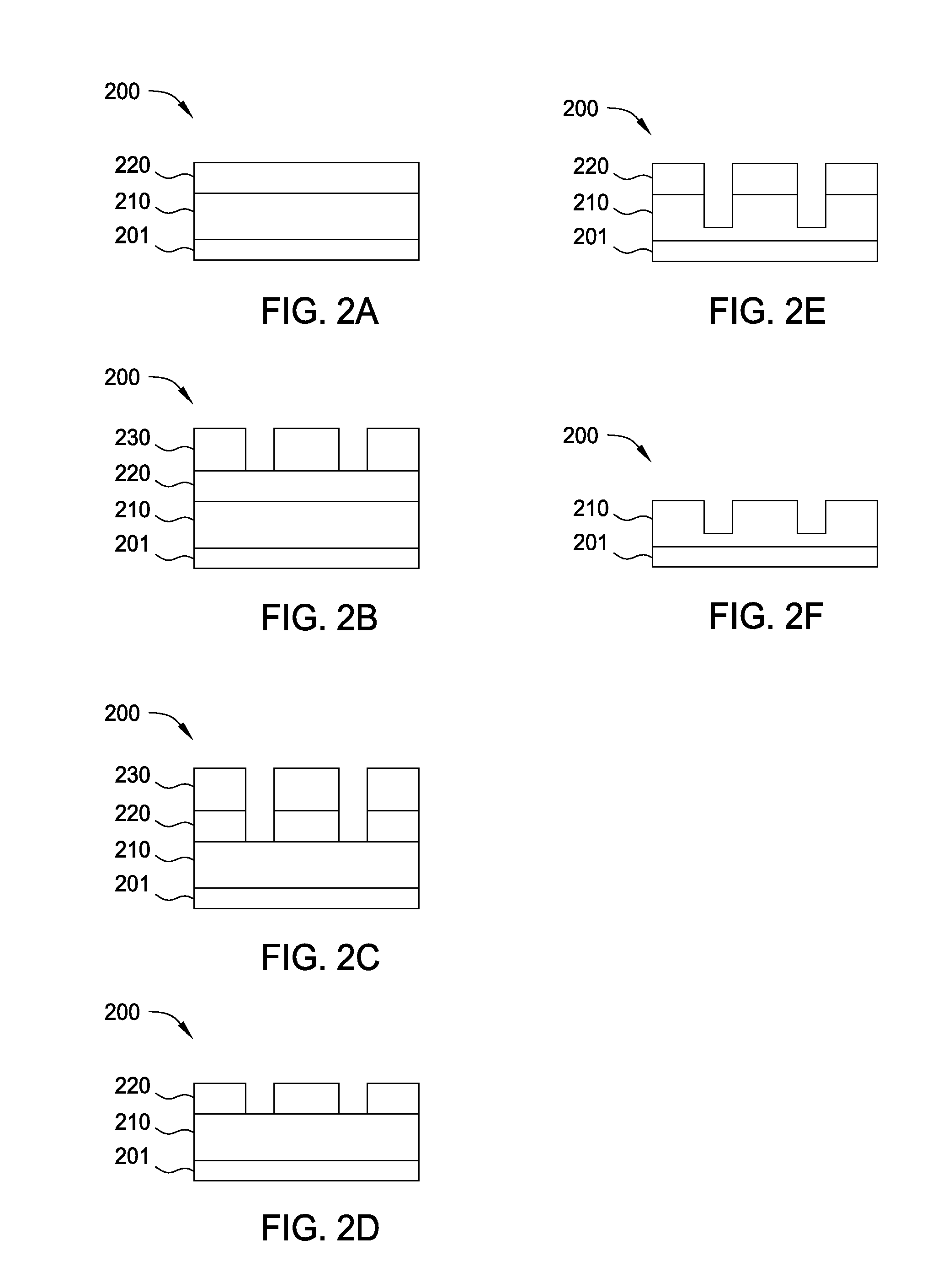
[0016]Embodiments disclosed herein generally provide a carbon-containing layer doped with a heteroatom, such as sulfur, phosphorous, nitrogen, oxygen, and / or fluorine. The heteroatom-doped carbon-containing layer may be used as a hardmask or in other applications. If the heteroatom-doped carbon-containing layer is used as a hardmask, the layer may be used to fabricate NAND devices, DRAM devices, or oth...


PUM

PropertyMeasurementUnit
pressureaaaaaaaaaa
pressureaaaaaaaaaa
temperatureaaaaaaaaaa

Abstract

Easily removable heteroatom-doped carbon-containing layers are deposited. The carbon-containing layers may be used as hardmasks. The heteroatom-doped carbon-containing hardmasks have high etch selectivity and density and also a low compressive stress, which will reduce or eliminate problems with wafer bow. Heteroatoms incorporated into the hardmask include sulfur, phosphorous, nitrogen, oxygen, and fluorine, all of which have low reactivity towards commonly used etchants. When sulfur is used as the heteroatom, the hardmask is easily removed, which simplifies the fabrication of NAND devices, DRAM devices, and other devices.

Description

BACKGROUND[0001]1. Field[0002]Embodiments of the present invention generally relate to a method and apparatus for fabricating a semiconductor device.[0003]2. Description of the Related Art[0004]Hardmasks are used to fabricate NAND and dynamic random access memory (DRAM) devices. Hardmasks are commonly used as sacrificial layers in lithographic patterning and enable, through an etching process, the patterning of features onto a layer of a semiconductor device. The patterned features can form, for example, the transistors and interconnects that allow the NAND and DRAM devices to operate.[0005]The important properties of a hardmask material are etch resistance, compressive stress, mechanical properties, and removability. An ideal hardmask has a high etch resistance compared to the layer to be etch (hereinafter, an “underlayer”) so that the underlayer etches in an etch process whereas the hardmask does not. A high etch resistance allows efficient transfer of the pattern of the hard mask...

Claims


Application Information

Patent Timeline
Patent Type & Authority Applications(United States)
IPC IPC(8): H01L21/027H01L21/311
CPCH01L21/31133H01L21/0271C23C16/402C23C16/45553H01L21/02115H01L21/02274H01L21/0332H01L21/31144Y10T428/24802
Inventor MANNA, PRAMITMALLICK, ABHIJIT BASUSRINIVASAN, MUKUND
Owner APPLIED MATERIALS INC
Why Eureka
Try Eureka