Semiconductor integrated circuit

Active Publication Date: 2015-07-23
WIN SEMICON
View PDF6 Cites 7 Cited by
  • Summary
  • Abstract
  • Description
  • Claims
  • Application Information

AI Technical Summary

Benefits of technology

[0005]The present invention provides a compound semiconductor integrated circuit chip having a front and/or back surface metal layer used for electrical connection to an external circuit. Its main object is to provide a semiconductor integrated circuit, which comprises stacked electronic chips, in which at least one of the chips is a compound semiconductor electronic integrated circuit chip. The footprint of a module composed of the semiconductor integrated circuit with stacked chips can be reduced significan

Problems solved by technology

The high integration of circuit elements induces high process cost and low process yield.
However, the use of multiple chips in

Method used


Image

  • Semiconductor integrated circuit
  • Semiconductor integrated circuit
  • Semiconductor integrated circuit

Examples


Example

Embodiment 1

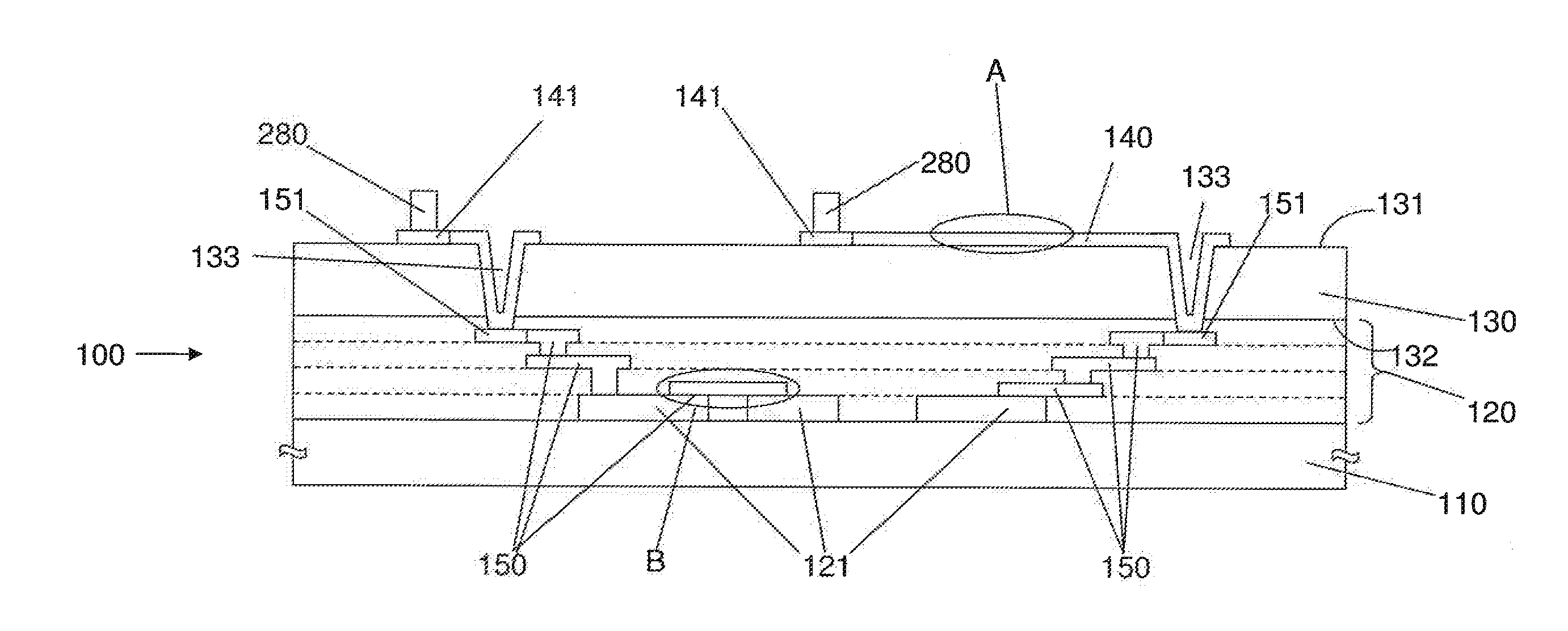
[0084]FIG. 5 is a schematic showing the cross-sectional view of another embodiment of the semiconductor integrated circuit according to the present invention, in which the first chip 100 contains an HEMT MMIC 103, and the second chip 200 contains an HBT power amplifier (PA) MMIC 203. The HEMT MMIC 103 has a substrate 110 made of GaAs. On the substrate 110 of the HEMT MMIC is an electronic device layer 120 consisting of bias control, switch, and logic circuits constructed by pseudomorphic HEMTs (pHEMTs) 121. The HEMT MMIC serves as a circuit to control the bias condition of the HBT PA and / or to control the RF signal path in the HBT PA. The electronic device layer 120 may contains one or more SiN layers for the insulation and passivation of the devices. On the HEMT MMIC, a dielectric layer 130 made of PBO is deposited on the surface as an insulating layer. The dielectric layer is spin coated to the thickness of about 10 μm. To provide electrical connection to the underlyin...

Example

Embodiment 2

[0085]FIG. 6 is a schematic showing the cross-sectional view of another embodiment of the semiconductor integrated circuit according to the present invention, in which the first chip 100 contains a HEMT MMIC 103 and the second chip 200 contains an HEMT PA MMIC 203. The HEMT MMIC 103 consists of bias control, switch, and logic circuits, and serves as a circuit to control the bias condition for the HEMT PA MMIC 203 and / or to control the RF signal path in the HEMT PA MMIC 203. Other descriptions about the design of this embodiment are the same as that of the embodiment 1, except that the HBT PA MMIC of the second chip 200 is replaced by the HEMT PA MMIC.

Example

Embodiment 3

[0086]FIG. 7 is a schematic showing the cross-sectional view of another embodiment of the semiconductor integrated circuit according to the present invention, in which the first chip 100 contains an HEMT MMIC 103 and the second chip 200 contains an HBT PA MMIC 203. The second chip 200 is stacked on the front surface 102 of the first chip 100 and the stacked chips are turned over and the second chip 200 is assembled on a module substrate 90 by wire bonding via bonding wires 204. Other descriptions about the design of this embodiment are the same as that of the embodiment 1


PUM


Abstract

The present invention relates to a compound semiconductor integrated circuit chip having a front and/or back surface metal layer used for electrical connection to an external circuit. The compound semiconductor integrated circuit chip (first chip) comprises a substrate, an electronic device layer, and a dielectric layer. A first metal layer is formed on the front side of the dielectric layer, and a third metal layer is formed on the back side of the substrate. The first and third metal layer are made essentially of Cu and used for the connection to other electronic circuits. A second chip may be mounted on the first chip with electrical connection made with the first or the third metal layer that extends over the electronic device in the first chip in the three-dimensional manner to make the electrical connection between the two chips having connection nodes away from each other.

Description

FIELD OF THE INVENTION[0001]The present invention relates to a semiconductor integrated circuit chip having a front and / or back surface metal layer used for electrical connection to an external circuit, and more particularly to a semiconductor integrated circuit with multiple stacked electronic circuit chips, in which at least one of them is a compound semiconductor MMIC chip.BACKGROUND OF THE INVENTION[0002]Compound semiconductor monolithic microwave integrated circuits (MMICs) have been widely used for the RF transmitter, receiver, and transceiver in microwave communication devices such as cell phones and wireless LAN modules. The RF modules are composed of many circuit elements such as power amplifiers (PAs), switches, filters, and control devices.[0003]Some of those circuit elements are integrated in one chip. A compound semiconductor amplifier (HBT or HEMT) often uses circuits using HEMTs for controlling the transistor bias condition. Those circuits can be integrated in one com...

Claims


Application Information

Patent Timeline
IPC IPC(8): H01L25/00H01L21/02H01L21/8234H01L25/18H01L21/8252H01L21/285H01L21/768
CPCH01L25/50H01L21/28568H01L21/0217H01L21/76802H01L21/8234H01L21/02118H01L25/18H01L21/76898H01L21/8252H01L21/76877H01L23/481H01L23/5223H01L23/5227H01L23/5228H01L23/53238H01L23/53252H01L23/66H01L29/737H01L25/0657H01L29/778H01L2223/6616H01L2223/6644H01L2223/6683H01L2224/16145H01L2224/32225H01L2224/48091H01L2224/48227H01L2224/73257H01L2224/73265H01L2225/0651H01L2225/06517H01L2924/1305H01L2223/6672H01L2225/06513H01L2225/06541H01L23/48H01L2924/00014H01L24/16H01L2224/05548H01L24/06H01L2224/06181H01L2224/17181H01L2224/73207H01L2224/16227H01L2224/02381H01L24/02H01L2224/0401H01L2224/05647H01L2224/05644H01L2224/05166H01L2224/05164H01L2224/05082H01L2224/05147H01L2224/05144H01L2224/13082H01L2224/13147H01L2224/13111H01L24/05H01L24/13H01L24/17H01L24/48H01L24/73H01L2224/05666H01L2924/00H01L2224/45015H01L2924/207H01L2224/45099H01L2924/01074H01L2924/01047H01L2224/16225
Inventor TAKATANI, SHINICHIROHSIAO, HSIEN-FULIN, CHENG-KUOHUA, CHANG-HWANG
Owner WIN SEMICON
Why Eureka
Try Eureka