

Antimony-Rich High-speed Phase-change Material Used In Phase-Change Memory, Preparing Method, And Application Thereof
a phase-change memory and antimony-rich technology, applied in the field of metal element-doped phase-change materials, can solve the problems of power consumption, block the wide application of material in the phase-change storage field, and the phase-change storage technology cannot show the competitive advantage, etc., to achieve the effect of accelerating the phase-change speed, and increasing the surface area/volume ratio
- Summary
- Abstract
- Description
- Claims
- Application Information
AI Technical Summary
Benefits of technology
Problems solved by technology
Method used
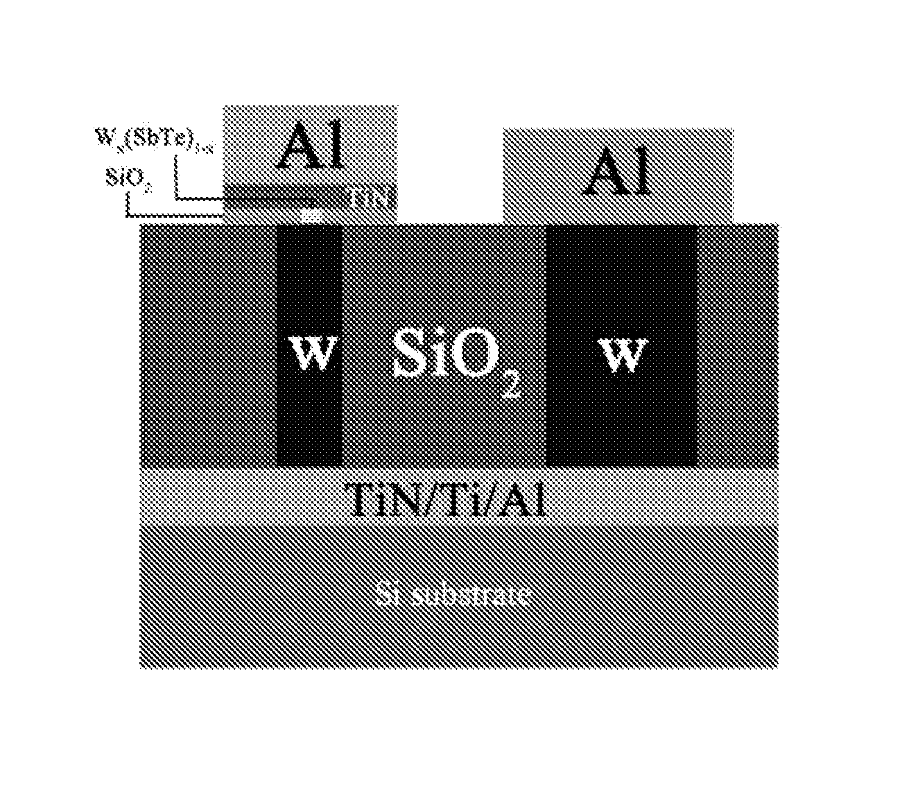
Image

Examples
embodiment 1
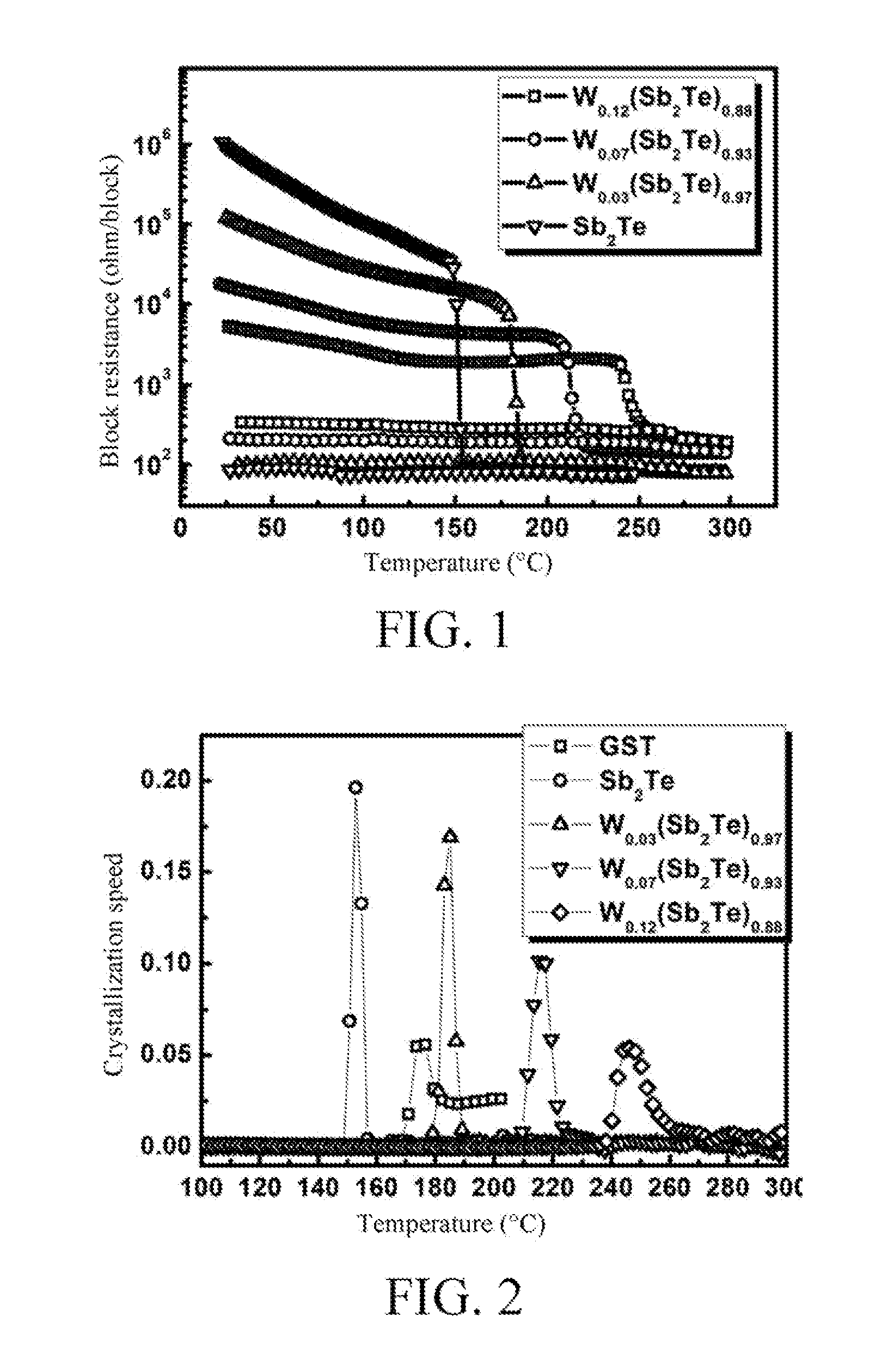
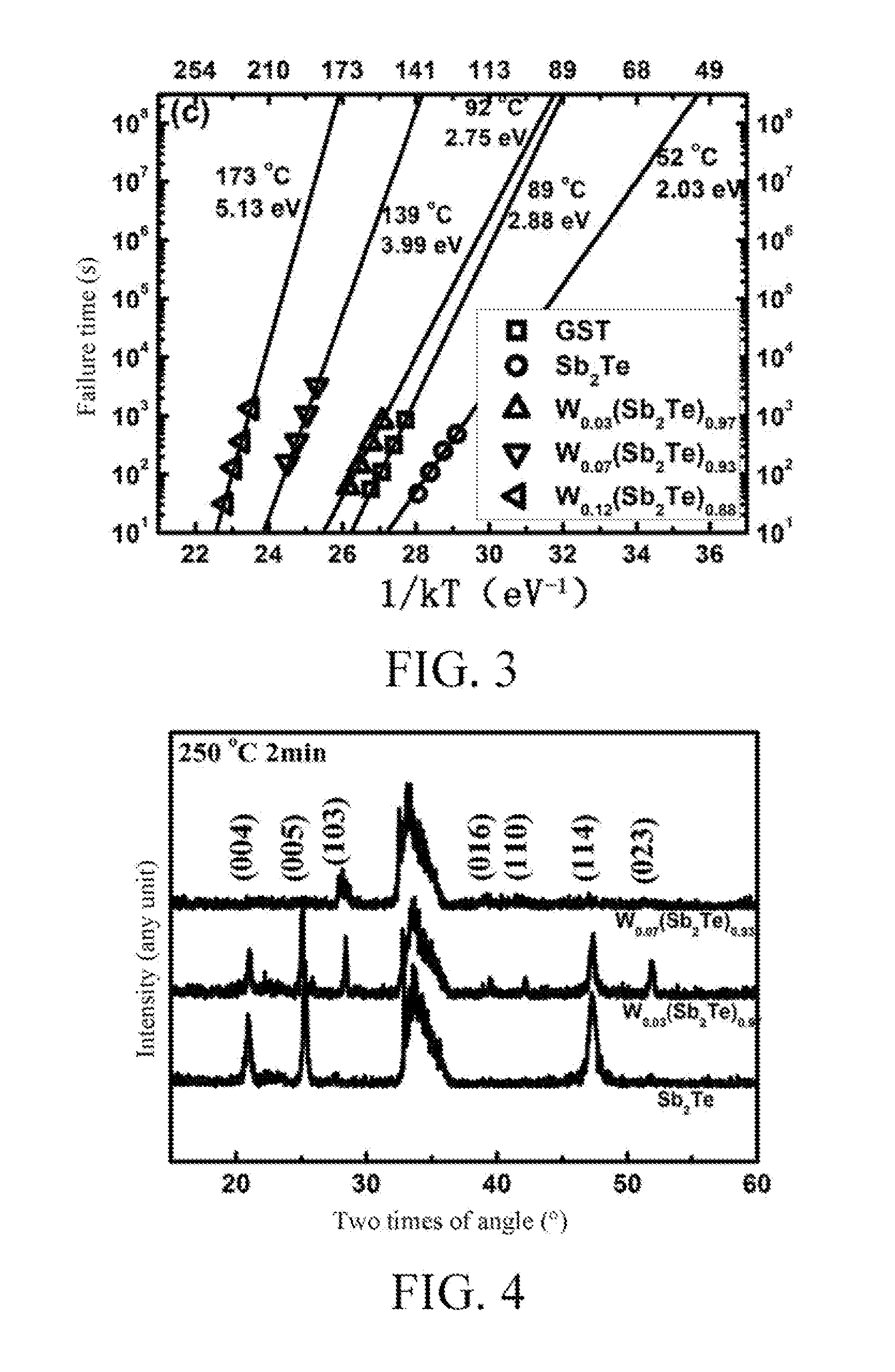
[0040]1. A Wx(Sb2Te)1−x thin film is prepared on a silicon substrate after being thermo-oxidized by using W and Sb2Te dual-target co-sputtering which belongs to magnetron sputtering, where during the co-sputtering, a background vacuum degree is 2.0×10⁻⁴ Pa, and an argon air pressure during sputtering is 0.22 Pa. A sputtering power of the Sb2Te target is fixed at RF 20 W, and sputtering powers of the W target are changed, respectively being RF 0 W, 5 W, 7 W, and 10 W, so as to obtain 4 types of phase-change thin films a#, b#, c#, and d# with different W doping concentrations. Parameters of the 4 types of phase-change thin films are shown in Table 1 in the following.
TABLE 1SampleFilm growing timeAtom percent x innumberSource power(min) / film thickness (nm)Wx(Sb2Te)1−xa#W: RF 0 W40 / 1590Sb2Te: RF 20 Wb#W: RF 5 W40 / 1540.03Sb2Te: RF 20 Wc#W: RF 7 W40 / 1390.07Sb2Te: RF 20 Wd#W: RF 10 W40 / 1490.12Sb2Te: RF 20 W
[0041]2. An original position resistance test is performed on the Wx(Sb2Te)1−x thin ...
embodiment 2
[0046]1. A Ti0.1(Sb2Te)0.9 thin film is prepared on a silicon substrate after being thermo-oxidized by using magnetron sputtering. A specific experiment method is that: single target sputtering is performed on prepared Ti0.1(Sb2Te)0.9, a power is RF 30 W, a background vacuum degree is 1.8×10⁻⁴ Pa, an argon air pressure during sputtering is 0.19 Pa, and a thin film thickness is 200 nm.
[0047]2. An original position resistance-temperature test is performed on the Ti0.1 (Sb2Te)0.9 thin film to obtain that a crystallization temperature is 225° C., and a data holding capability is calculated to be 137° C., where both of the two values are much higher than that of the Ge2Sb2Te5 thin film.
[0048]3. A voltage change of the Ti0.1(Sb2Te)0.9 thin film before and after the phase-change is quite small, distribution of crystal grains are quite uniform, and phase splitting does not exist, so the Ti0.1 (Sb2Te)0.9 thin film is quite suitable to be used in a high-speed and high-density memory.
PUM
| Property | Measurement | Unit |
|---|---|---|
| Length | aaaaa | aaaaa |
| Pressure | aaaaa | aaaaa |
| Pressure | aaaaa | aaaaa |
Abstract
Description
Claims
Application Information