MEMS pressure sensor with improved insensitivity to thermo-mechanical stress

a technology of thermo-mechanical stress and pressure sensor, which is applied in the direction of fluid pressure measurement, fluid pressure measurement by electric/magnetic elements, instruments, etc., can solve the problems of non-uniform stress within the substrate, non-uniform stress may be accumulated in the mems device, and offset or sensitivity drift, etc., to achieve the effect of increasing pressure insensitivity and improving pressure sensor performan

Active Publication Date: 2015-10-01
HANKING ELECTRONICS LTD
View PDF14 Cites 13 Cited by
  • Summary
  • Abstract
  • Description
  • Claims
  • Application Information

AI Technical Summary

Benefits of technology

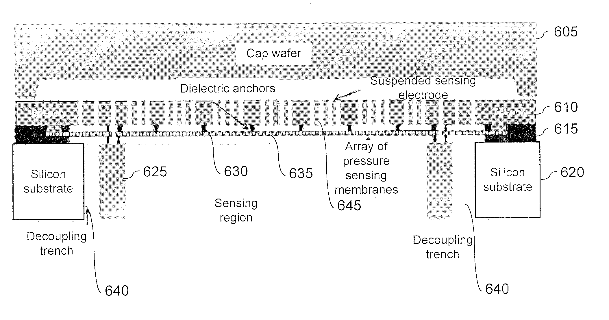
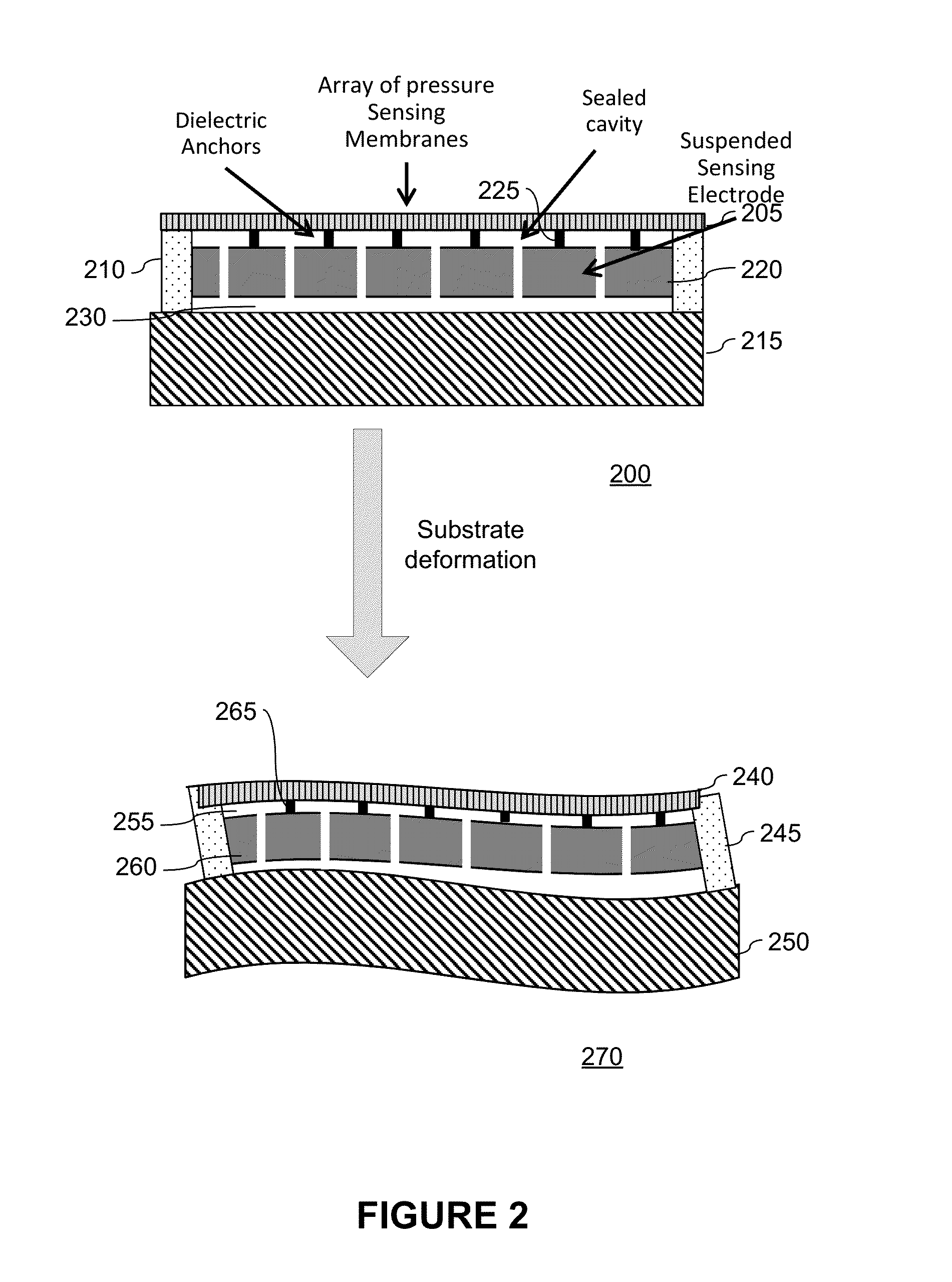
[0014]This invention relates generally to semiconductor manufacturing and packaging and more specifically to semiconductor manufacturing in MEMS (Microelectromechanical systems) sensing products. Embodiments of the present invention improve pressure sensor performance (e.g., absolute and relative accuracy) by increasing pressure insensitivity to changes in thermo-mechanical stress. The pressure insensitivity can be achieved by using the array of pressure sensing membranes, suspended sensing electrodes, and dielectric anchors.
[0015]Embodiments of the present invention improve pressure sensor performance (e.g., absolute and relative accuracy) by increasing pressure insensitivity to changes in thermo-mechanical stress.
[0016]In one embodiment the thermo-mechanical insensitivity is achieved using an array of pressure sensing membranes, a sealed cavity, suspended sensing electrodes, and dielectric anchors. By suspending the pressure sensors the impact of substrate deformation is reduced.
[0017]Another benefit of this innovation is it easily enabled integration in the same die of pressure sensor and other inertial sensors.

Problems solved by technology

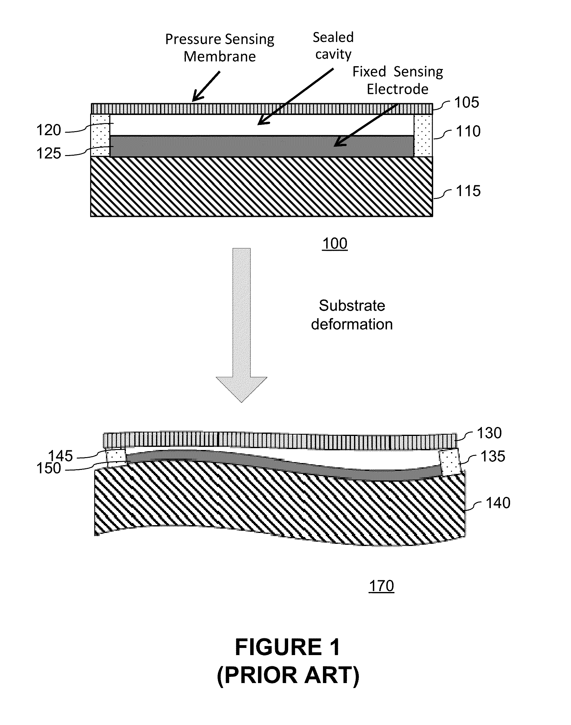
Thermo-mechanical stress may produce deformation of both electrodes in different way, and ultimately, lead to an offset or sensitivity drift to the sensing capacitor (sensor interface circuit) even though no pressure difference is applied to induce any capacitive change.
However, thermo-mechanical stress may be accumulated in the MEMS device during the course of manufacturing, soldering, packaging and device aging.
Non-uniform stress can build up within the substrate and the device structure including the membrane, and unavoidably cause the substrate to warp and the membrane to shift or to be deformed.
The sensing output from a sensor interface circuit may reflect such displacements resulting from the non-uniform thermal stress, and lead to an offset value and a sensitivity drift for the sensed pressure.
Device performance of a capacitive pressure sensor is compromised due to the thermo-mechanical stress.
However, this method still produces inaccuracies and increases complexity and cost of the package itself.
On this kind of device when a substrate deformation due to package stress or temperature occurs, capacitance variation due to undesired fixed electrode or membrane deformation can be detected even without applied pressure, causing loss in sensor accuracy.

Method used


Image

  • MEMS pressure sensor with improved insensitivity to thermo-mechanical stress
  • MEMS pressure sensor with improved insensitivity to thermo-mechanical stress
  • MEMS pressure sensor with improved insensitivity to thermo-mechanical stress

Examples


Embodiment Construction

[0027]The following description is set forth for purpose of explanation in order to provide an understanding of the invention. However, it is apparent that one skilled in the art will recognize that embodiments of the present invention, some of which are described below, may be incorporated into a number of different systems and devices. The embodiments of the present invention may be present in hardware, software or firmware. Structures shown below in the diagram are illustrative of exemplary embodiments of the invention and are meant to avoid obscuring the invention. Furthermore, connections between components within the figures are not intended to be limited to direct connections. Rather, data between these components may be modified, re-formatted or otherwise changed by intermediary components.

[0028]Reference in the specification to “one embodiment”, “in one embodiment” or “an embodiment” etc. means that a particular feature, structure, characteristic, or function described in c...


PUM

PropertyMeasurementUnit
thermo-mechanical insensitivityaaaaaaaaaa
dielectricaaaaaaaaaa
pressureaaaaaaaaaa

Abstract

This invention relates generally to semiconductor manufacturing and packaging and more specifically to semiconductor manufacturing in MEMS (Microelectromechanical systems) inertial sensing products. Embodiments of the present invention improve pressure sensor performance (e.g., absolute and relative accuracy) by increasing pressure insensitivity to changes in thermo-mechanical stress. The pressure insensitivity can be achieved by using the array of pressure sensing membranes, suspended sensing electrodes, and dielectric anchors.

Description

CROSS REFERENCE TO RELATED APPLICATIONS[0001]This application claims the benefit of U.S. Provisional Application No. 61 / 971,393, filed Mar. 27, 2014.BACKGROUND[0002]A. Technical Field[0003]This invention relates generally to semiconductor manufacturing and packaging and more specifically to semiconductor manufacturing in MEMS (Microelectromechanical systems) sensing products.[0004]B. Background of the Invention[0005]A microelectromechanical structure (MEMS) is widely applied as a sensor to measure acceleration, rotation, pressure and many other physical parameters. The MEMS device is normally formed on a silicon substrate using a micromachining process, and thus, adopts characteristic feature sizes of several micrometers. Such miniaturized devices transduce mechanical movement to electrical signals that may indicate the level of the interested parameters. Examples of the MEMS device include accelerometers, gyroscopes, magnetometers, and pressure sensors. Various MEMS devices have be...

Claims


Application Information

Patent Timeline
Patent Type & Authority Applications(United States)
IPC IPC(8): B81B3/00B81C1/00
CPCB81B3/0078B81B2203/0127B81B2201/0264B81C1/00682B81B7/0054B81B2203/04G01L9/0073G01L9/00
Inventor MOLFESE, ANTONIOCORONATO, LUCACAZZANIGA, GABRIELEESPOSITO, LUIGI
Owner HANKING ELECTRONICS LTD
Why Eureka
Try Eureka