Semiconductor photosensor for infrared radiation

a technology of infrared radiation and semiconductors, applied in the direction of optical radiation measurement, radiation control devices, instruments, etc., can solve the problems of limited number of photosensing elements, limited sensitivity of microbolometers, and inability to come close to single-photon sensitivity

Active Publication Date: 2015-10-01
HAMAMATSU PHOTONICS KK
View PDF4 Cites 8 Cited by
  • Summary
  • Abstract
  • Description
  • Claims
  • Application Information

AI Technical Summary

Benefits of technology

[0020]This invention may provide a photosensor for the highly sensitive

Problems solved by technology

Because of the difficulty of processing most pyroelectric materials, only limited numbers of photosensing elements (pixels) are fabricated on a single detector device, typically between one and several hundred pixels.
However, because their working principle depends on device heating, the sensitivity of microbolometers is quite restricted, and it is impossible to come close to single-photon sensitivity.
The cutoff wavelength λC is inversely proportional to the minimum energy Emin, required to create mobile charge carriers due to the photoeffect, λC=h×c/Emin, with Planck's constant h and the vacuum speed of light c. This implies that the photoelectric effect is unsuitable for the detection of electromagnetic radiation in the infrared spectral range with its particularly long wavelengths.
However, HIP infrared photosensors suffer from two

Method used


Image

  • Semiconductor photosensor for infrared radiation
  • Semiconductor photosensor for infrared radiation
  • Semiconductor photosensor for infrared radiation

Examples


Embodiment Construction

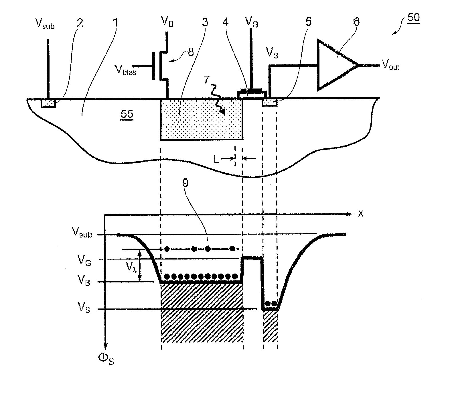
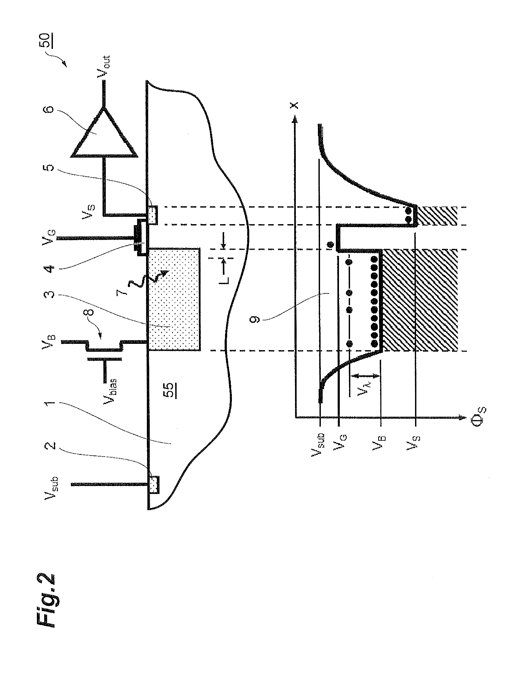
[0032]It is a principle object of the invention to provide a photosensor for the highly sensitive detection of infrared radiation in the wide spectral range from 1 to 1000 micrometers.

[0033]A further object of the invention is to provide an infrared photosensor that can be fabricated with industry-standard semiconductor processes such as the widely available silicon-based CMOS processes.

[0034]Another object of the invention is to provide an infrared photosensor whose cutoff wavelength can be chosen fast and adaptively with a voltage.

[0035]Yet another object of the invention is to provide an infrared photosensor device with such a small footprint that one- and two-dimensional infrared image sensors can be created using industry-standard semiconductor processes, resulting for example in an infrared image sensor with at least one Megapixels per square centimeter.

[0036]A final object of the invention is to provide a photosensor device that can distinguish between photocurrents generated...


PUM


Abstract

A photosensor for the detection of infrared radiation in the wavelength range of 1 to 1000 micrometers consists of a semiconductor substrate with a highly doped interaction volume for the incoming radiation. At the edge of this highly doped region, an extended gate electrode is placed consisting of a conducting material on top of an insulating layer. On the other side of the gate electrode, another highly doped semiconductor region is placed, acting as a charge collector. Through free carrier absorption in the interaction volume, incoming photons impart their energy on mobile charge carriers. In the case of free electrons, the gate electrode is biased slightly below the reset voltage of the interaction volume, so that the electrons carrying the additional energy of the absorbed photons can predominantly make the transition from the interaction volume across the gate electrode area to the charge collector volume.

Description

TECHNICAL FIELD[0001]The present invention relates to a method and a device for the detection of infrared radiation in the wavelength range of 1 to 1000 micrometers, making use of known semiconductor manufacturing processes. In particular, the invention relates to an infrared photosensor that can be manufactured with silicon processes such as the ones widely used for silicon-based CMOS (Complementary Metal Oxide Semiconductor) devices.BACKGROUND ART[0002]The detection of electromagnetic radiation is one of the most important sensing tasks in science, technology and consumer electronics. Silicon is the fundamental semiconductor of microelectronics, and it is very well suited for the fabrication of highly sensitive photosensors—from point detectors to multi-megapixel image sensors—covering the wide spectral domain from the soft X-ray region to the near infrared. This corresponds to a sensitive wavelength range from about 1 nm up to the cutoff-wavelength of silicon of about 1100 nm. Du...

Claims


Application Information

Patent Timeline
IPC IPC(8): H01L31/113G01J5/24H01L27/146
CPCH01L31/1136G01J5/24H01L27/14649H01L31/02027H01L31/103H01L31/02019H01L31/1037G01J1/46
Inventor SEITZ, PETER
Owner HAMAMATSU PHOTONICS KK
Why Eureka
Try Eureka