EMI shielded wafer level fan-out pop package

a technology of shielding wafers and pop packages, applied in the field of shielding packageonpackage, can solve the problems of poor thermal conduction between the components of the package, hysteresis losses, and electromagnetic field around the conductor is no longer evenly distributed, and achieves enhanced emi attenuation and reflectance, high permeability difference, and high emi shield effectiveness.

Active Publication Date: 2015-10-22
APPLE INC
View PDF2 Cites 12 Cited by
  • Summary
  • Abstract
  • Description
  • Claims
  • Application Information

AI Technical Summary

Benefits of technology

[0010]In some embodiments, an EMI self-shielded wafer level PoP structure is provided that provides high EMI shield effectiveness. In some embodiments, EMI self-shielding may be achieved by coating conductive material over the surface of the PoP package. The coating material may be applied by processes such as sputter / CVD / spray / etc. The high electrically conductive coating layer may consist of multiple layers having high permeability difference between adjacent layers that enhance EMI attenuation and reflectance. The shielding layer may be electrically connected to a redistribution layer, ground terminals, vias, or traces that are engineered to be exposed at the package side surface. In some embodiments, a metal lid applied on top of PoP for thermal enhancement purpose may be partially or fully connected to the shielding layer, and further enhances EMI shielding performance.

Problems solved by technology

However, air is known as a very good insulator and as such results in poor thermal conduction between the components of the package.
Mutual inductance between two radiated electromagnetic fields may result in EMI.
Due to EMI, the electromagnetic field around the conductor is no longer evenly distributed (e.g., resulting in skin effects, proximity effects, hysteresis losses, transients, voltage drops, electromagnetic disturbances, EMP / HEMP, eddy current losses, harmonic distortion, and reduction in the permeability of the material).
The chips on these boards are so close to each other that the chances of conducted and radiated EMI are significant.
Technological advancements have drastically reduced the size of chipboards and electronics; however, this means they are also much more sensitive to EMI.
However, EMI shielding can be expensive and may have negative consequences.

Method used


Image

  • EMI shielded wafer level fan-out pop package
  • EMI shielded wafer level fan-out pop package
  • EMI shielded wafer level fan-out pop package

Examples


Embodiment Construction

[0027]This specification includes references to “one embodiment” or “an embodiment.” The appearances of the phrases “in one embodiment” or “in an embodiment” do not necessarily refer to the same embodiment. Particular features, structures, or characteristics may be combined in any suitable manner consistent with this disclosure.

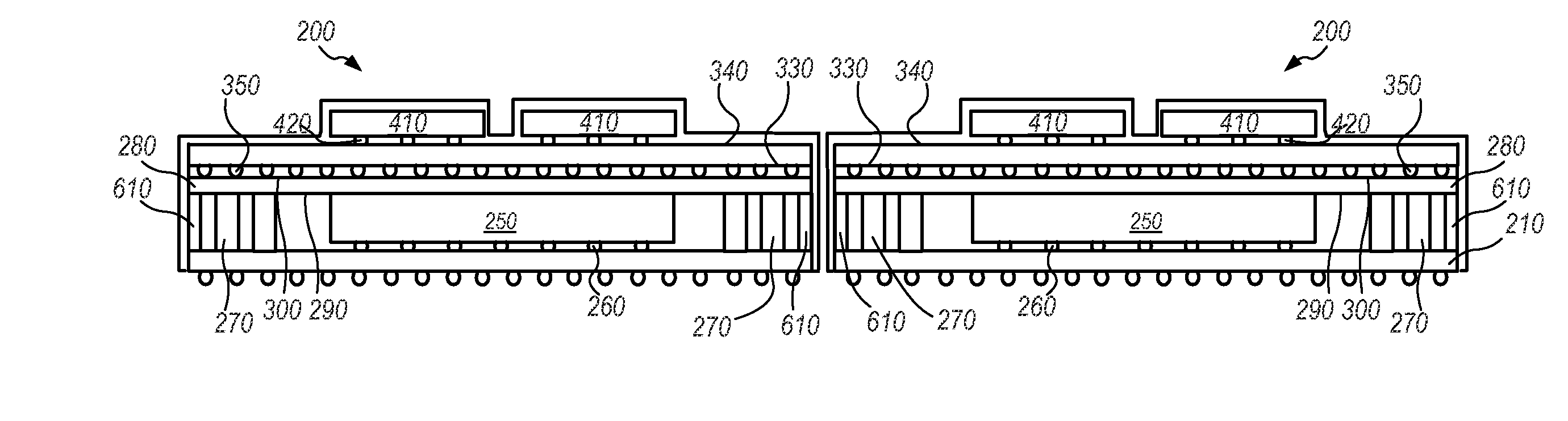
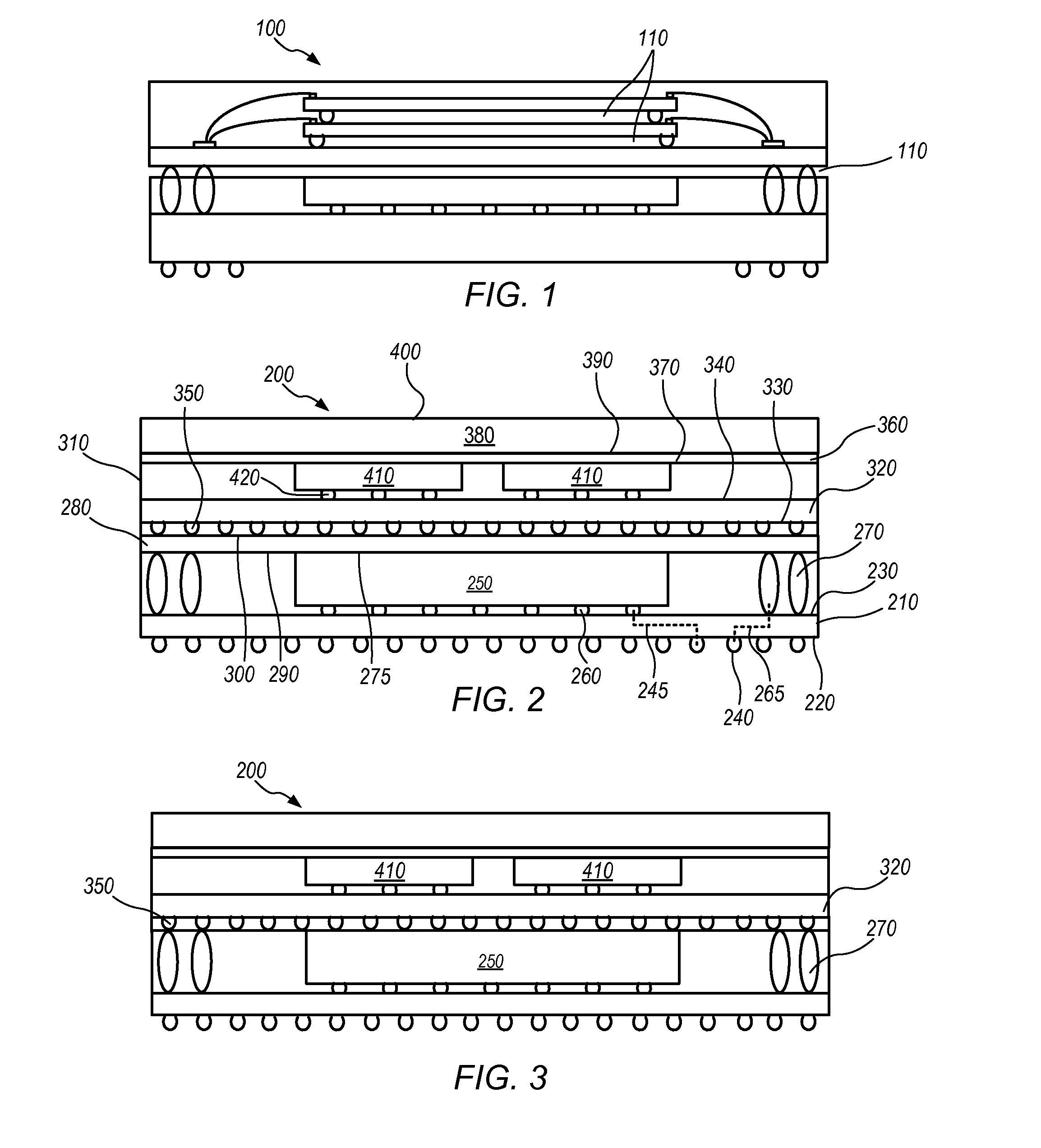
[0028]FIG. 2 depicts an embodiment of a thermally enhanced package on package format 200 including two redistribution layers. At least some of the electrical conductors are not depicted for the sake of clarity. In some embodiments, a semiconductor device package assembly 200 may include a first substrate 210 (or a first redistribution layer) including a first surface 220, a second surface 230 substantially opposite of the first surface, and a first set of electrical conductors 240 coupled to the first surface. The first set of electrical conductors may function to electrically connect the semiconductor device package assembly to, for example, other electrical...


PUM


Abstract

In some embodiments, a semiconductor device package assembly may include a first substrate. The first substrate may include a first set of electrical conductors which electrically connect the assembly. In some embodiments, the assembly may include at least one electrical conductor coupled to the first substrate such that at least one of the electrical conductors exposes through a perimeter surface of the semiconductor device package assembly. In some embodiments, the assembly may include a first die electrically connected to a second surface of the first substrate using a second set of electrical conductors. The assembly may include an electronic memory module coupled to the first die. In some embodiments, the assembly may include a shield applied to an upper surface of the assembly and electrically coupled to at least one of the exposed electrical conductors. The shield may inhibit, during use, electromagnetic interference.

Description

PRIORITY CLAIM[0001]This application claims priority to U.S. Provisional Patent Application No. 61 / 980,830 entitled “EMI SHIELDED WAFER LEVEL FAN-OUT POP PACKAGE” to Zhai et al. filed on Apr. 17, 2014, all of which is incorporated by reference herein.BACKGROUND[0002]1. Technical Field[0003]Embodiments described herein relate to semiconductor packaging and methods for packaging semiconductor devices. More particularly, some embodiments disclosed herein relate to shielding package-on-package (“PoP”) from electromagnetic interference.[0004]2. Description of the Related Art[0005]Package-on-package (“PoP”) technology has become increasingly popular as the demand for lower cost, higher performance, increased integrated circuit density, and increased package density continues in the semiconductor industry. As the push for smaller and smaller packages increases, the integration of die and package (e.g., “pre-stacking” or the integration of system on a chip (“SoC”) technology with memory tec...

Claims


Application Information

Patent Timeline
Patent Type & Authority Applications(United States)
IPC IPC(8): H01L23/552H01L23/367H01L25/18H01L23/00H01L25/00H01L25/065
CPCH01L23/552H01L2224/32245H01L25/0652H01L25/18H01L24/17H01L23/3675H01L24/81H01L2924/01029H01L2924/1434H01L2225/06517H01L2225/06513H01L2225/06589H01L2224/16145H01L2224/16225H01L25/50H01L23/367H01L23/49805H01L23/49811H01L21/561H01L24/97H01L25/0655H01L25/105H01L2224/73253H01L2224/97H01L23/3128H01L2225/1023H01L2225/06537H01L2924/15311H01L25/0657H01L24/32H01L2224/73257H01L2225/1094H01L2225/0651H01L2224/0401H01L2225/1041H01L2225/1058H01L2924/15331H01L2924/18161H01L24/73H01L24/16H01L2224/81
Inventor ZHAI, JUNPANG, MENGZHIYANG, SE YOUNGLEW, LELAND W.
Owner APPLE INC
Why Eureka
Try Eureka