Cigs film production method, and cigs solar cell production method using the cigs film production method
a technology of cigs film and production method, which is applied in the direction of sustainable manufacturing/processing, final product manufacture, vacuum evaporation coating, etc., can solve the problems of uniform diffusion of cu into the film, adversely affecting the characteristics of solar cells, and uniform crystal grains, etc., to achieve excellent conversion efficiency and advantageous control of the composition of the cigs film
- Summary
- Abstract
- Description
- Claims
- Application Information
AI Technical Summary
Benefits of technology
Problems solved by technology
Method used
Image
Examples
example 1
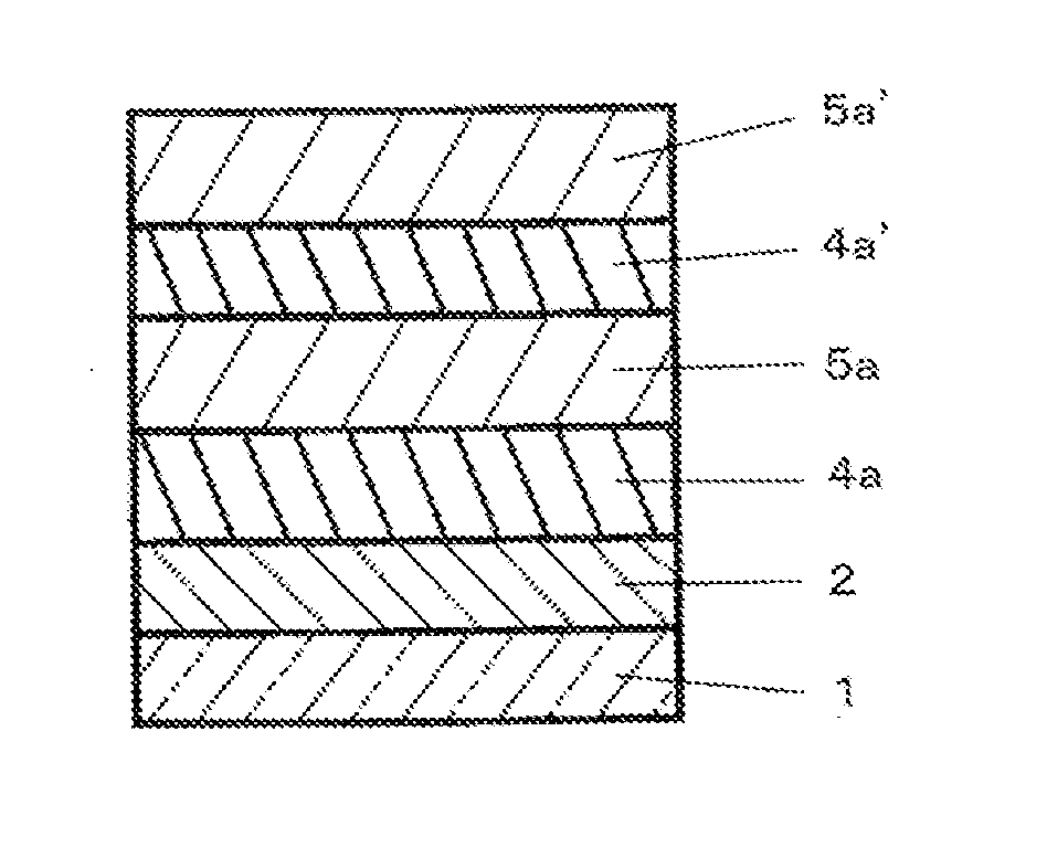
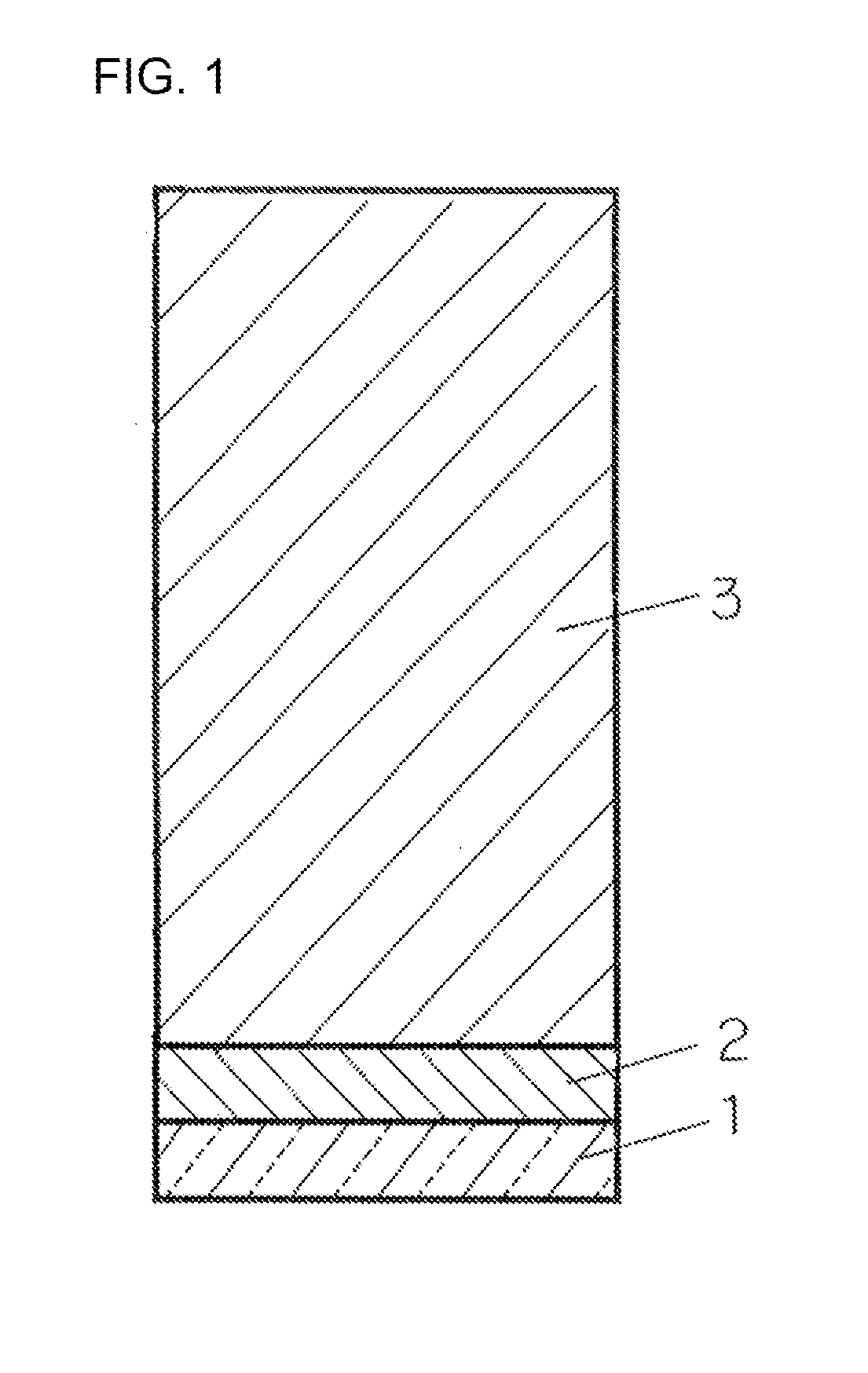
[0081]A CIGS solar cell was produced in the same manner as in the embodiment described above. More specifically, a SLG substrate (having a size of 30×30 mm and a thickness of 0.55 mm) was prepared, and Mo was deposited (to a thickness of 500 nm) over the substrate to form a rear electrode layer. While the substrate was maintained at a retention temperature of 200° C., a layer (A) was formed over the rear electrode layer under the following conditions.
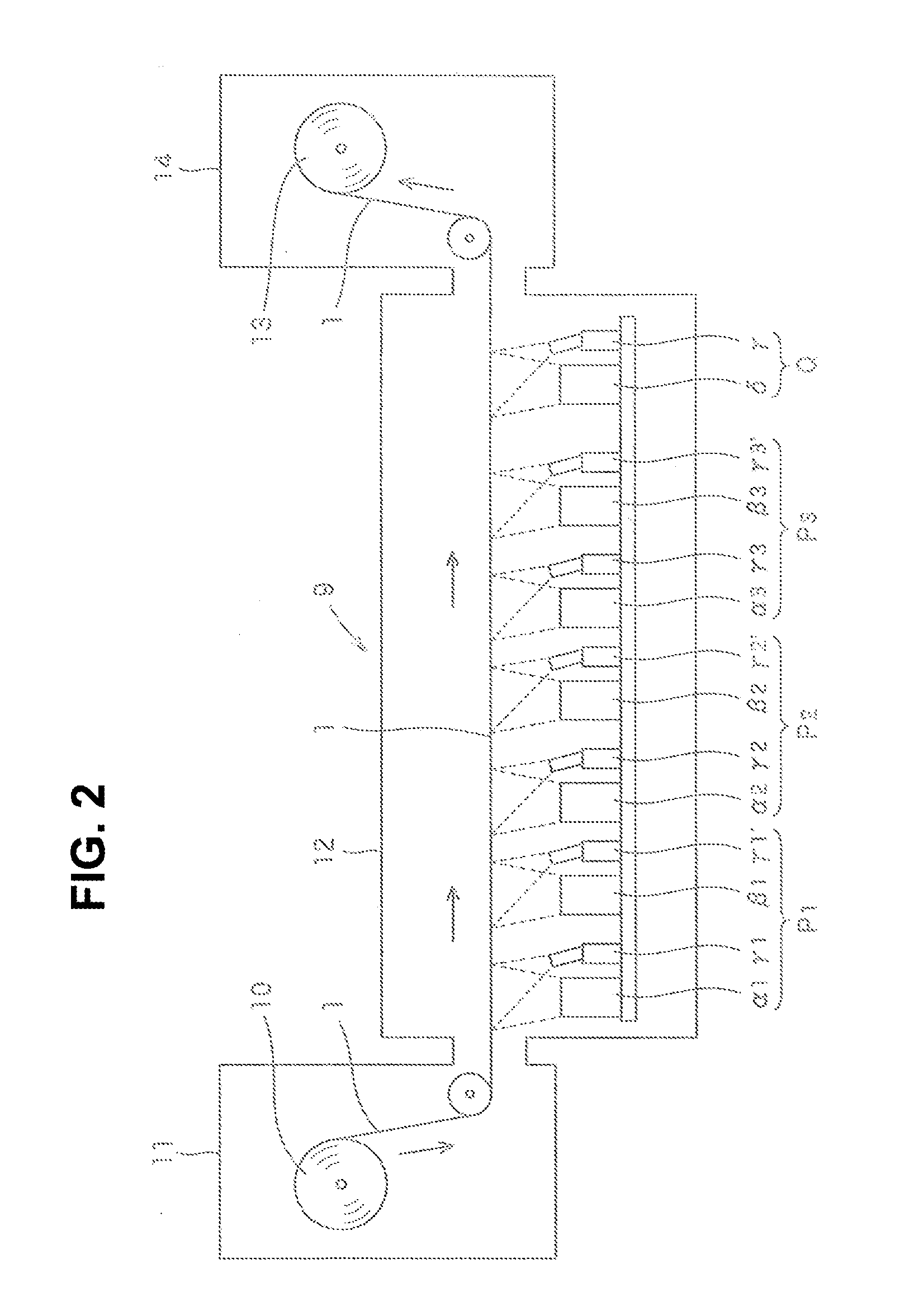
[0082]With the use of substantially the same apparatus as the evaporation apparatus 9 shown in FIG. 2, a gallium selenide film (Y) was first formed while the temperature of a Ga evaporation source was controlled at 1000° C. and the temperature of a Se evaporation source was controlled at 180° C. Then, an indium selenide film (X) was formed while the temperature of an In evaporation source was controlled at 850° C. and the temperature of the Se evaporation source was controlled at 180° C. Thus, the gallium selenide film (Y) and the indiu...
example 2
[0085]A CIGS solar cell of Example 2 was produced in substantially the same manner as in Example 1, except that the number of times of the stacking of the gallium selenide film (Y) and the indium selenide film (x) and the temperatures of the Ga evaporation sources for the respective stacking operations were changed as shown below in Table 2 for the formation of the layer (A) and the layer (C). The times required for the formation of the respective films were reduced so that the CIGS film had the same thickness as in Example 1.
PUM
| Property | Measurement | Unit |
|---|---|---|
| Temperature | aaaaa | aaaaa |
| Temperature | aaaaa | aaaaa |
| Temperature | aaaaa | aaaaa |
Abstract
Description
Claims
Application Information


