

Cigs film production method, and cigs solar cell production method using the cigs film production method
a technology of solar cells and film, applied in the field of cigs solar cell production method using cigs film production method, can solve the problems of uniform diffusion of adverse influence of solar cell characteristics, and inability to uniformly diffuse cu into the film, so as to achieve excellent conversion efficiency and reduce costs
- Summary
- Abstract
- Description
- Claims
- Application Information
AI Technical Summary
Benefits of technology
Problems solved by technology
Method used
Image

Examples
example 1
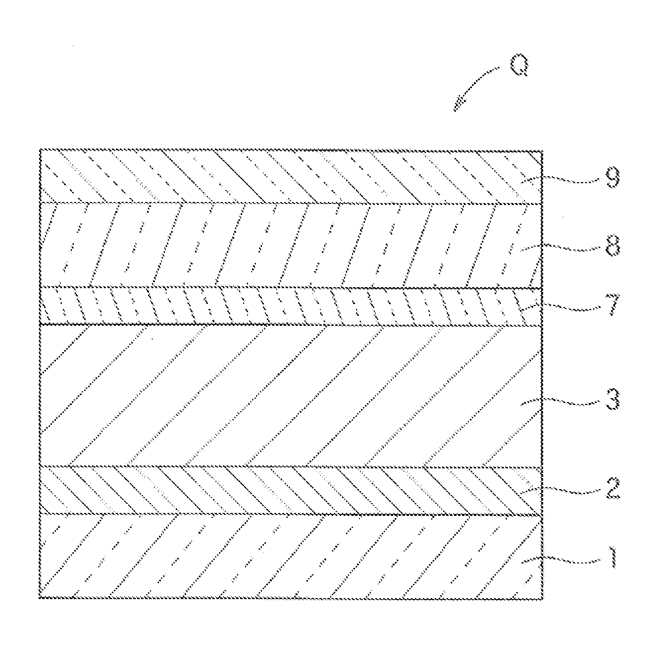
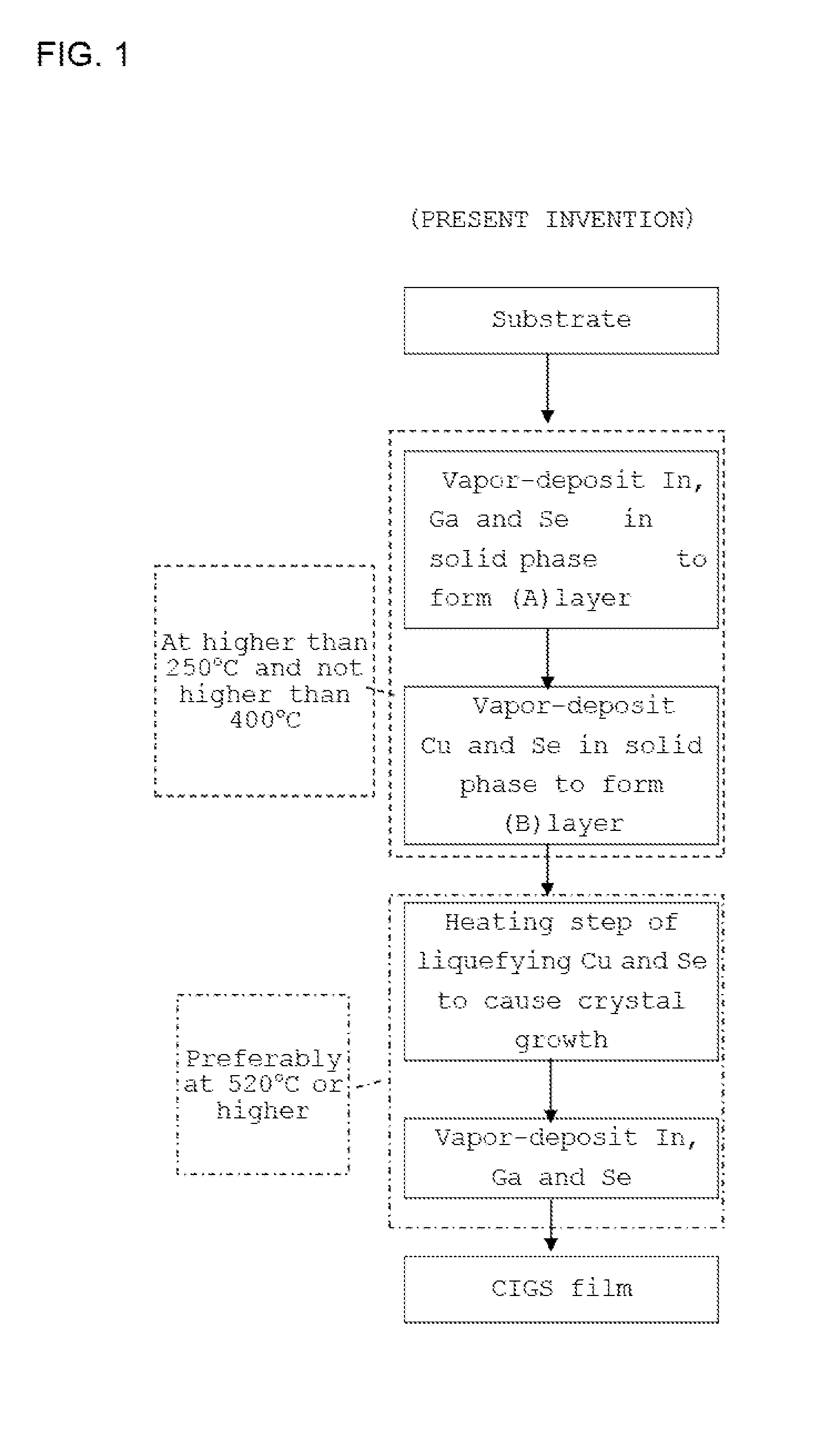
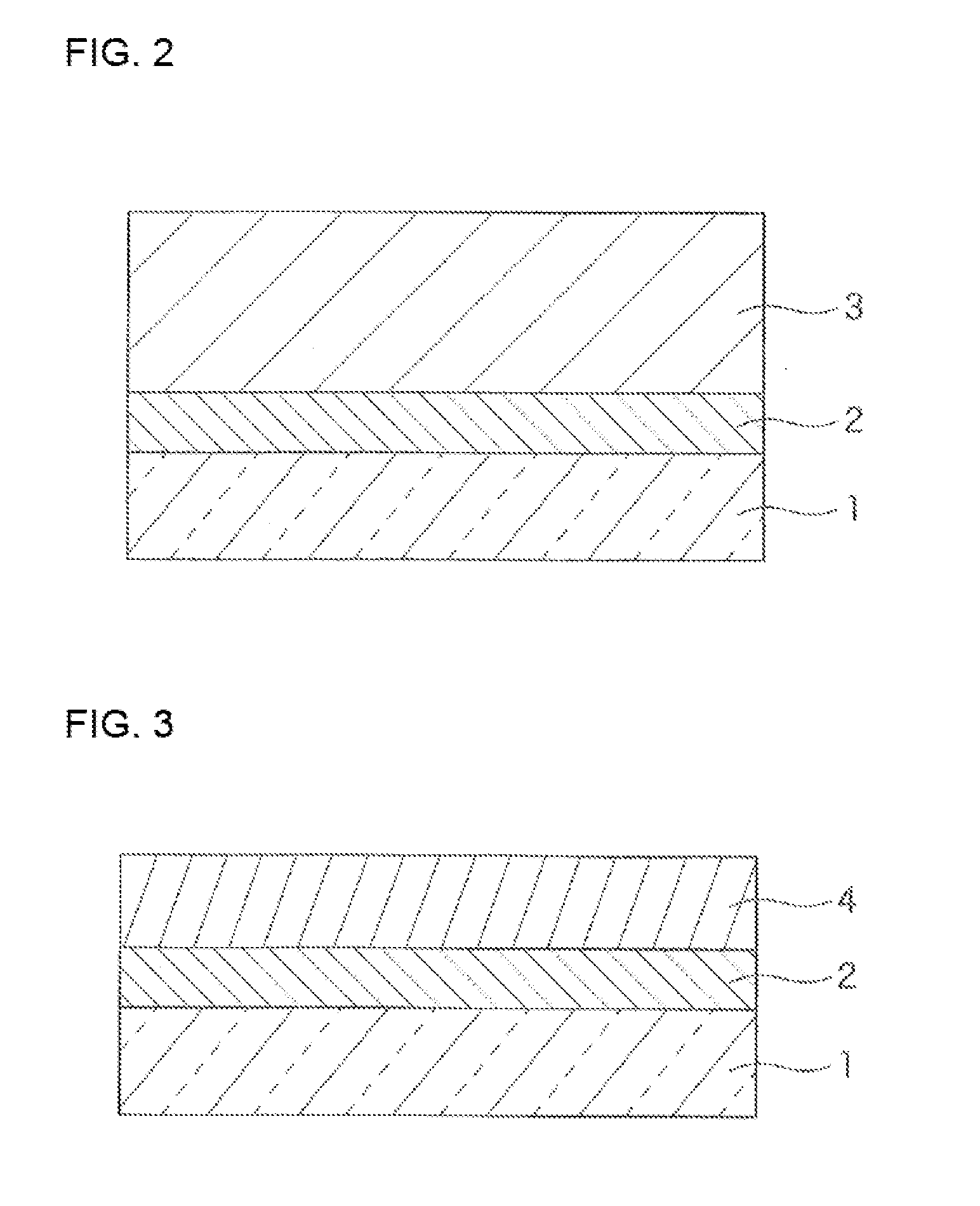
[0055]A CIGS solar cell was produced in the same manner as in the embodiment described above. More specifically, a SLG substrate (having a size of 30×30 mm and a thickness of 0.55 mm) was prepared as a substrate 1, and Mo was deposited (to a thickness of 500 nm) over the substrate 1 to form a rear electrode layer 2. While the substrate 1 was maintained at a retention temperature of 255° C., In, Ga and Se were vapor-deposited to form an (A) layer. In turn, with the substrate 1 maintained at a retention temperature of 255° C., Cu and Se were vapor-deposited on the (A) layer to form a (B) layer. Thus, a stack 6 was formed. While a very small amount of Se vapor was supplied to the stack 6, the substrate 1 was heated to be maintained at a retention temperature of 550° C. for 15 minutes to cause crystal growth. Thus, a CIGS film 3′ was produced. While a very small amount of Se gas was supplied to the CIGS film 3′ with the substrate 1 maintained at a retention temperature of 550° C., In, G...
PUM
 Abstract
Description
Claims
Application Information