Method for manufacturing gas barrier film, gas barrier film and electronic device

a technology of gas barrier film and electronic device, which is applied in the direction of magnetic materials, water-setting substance layered products, magnetic bodies, etc., can solve the problems of insufficient gas barrier film performance, insufficient gas barrier property, insufficient adhesion property and flexibility of electronic devices such as organic el elements, etc., to achieve excellent adhesion property, high flexibility, and superior gas barrier properties

Inactive Publication Date: 2016-02-18
KONICA MINOLTA INC
View PDF0 Cites 17 Cited by
  • Summary
  • Abstract
  • Description
  • Claims
  • Application Information

AI Technical Summary

Benefits of technology

[0010]One or more embodiments of the present invention provide a production method of a gas barrier film having a gas barrier property required for an electronic device application under the using condition of high temperature and high humidity such as an outdoor usage, as well as having high flexibility and excellent adhesion property. One or more embodiments of the present invention also provide a gas barrier film and an electronic device using the same.
[0011]The present inventors have found out a production method of a gas barrier film. According to one or more embodiments, the method comprises the steps of: forming a smoothing layer on one surface of a resin substrate, the smoothing layer having a surface free energy within a specific range at an environment of 23° C. and 50% RH; and forming a gas barrier layer containing a carbon atom, a silicon atom and an oxygen atom as constituting elements on a surface of the smoothing layer with a discharge plasma chemical vapor phase deposition method using a film forming gas containing an organic silicon compound as a raw material gas and an oxygen gas. By using this method, it can realize a production method of a gas barrier film having a gas barrier property required for an electronic device application under the using condition of high temperature and high humidity such as an outdoor usage, as well as having high flexibility and excellent adhesion property. Thus, the present invention has been achieved.

Problems solved by technology

However, with respect to these flexible electronic devices, it is required an extremely high gas barrier property comparable to a glass substrate level.
At present time, it has not been achieved a gas barrier film having sufficient performance.
However, it was found that its gas barrier property, adhesion property and flexibility for an electronic device such as an organic EL element were insufficient when used under the severe conditions of high temperature and high humidity such as an outdoor usage.

Method used


Image

  • Method for manufacturing gas barrier film, gas barrier film and electronic device
  • Method for manufacturing gas barrier film, gas barrier film and electronic device
  • Method for manufacturing gas barrier film, gas barrier film and electronic device

Examples


example 1

Preparation of Resin Substrate

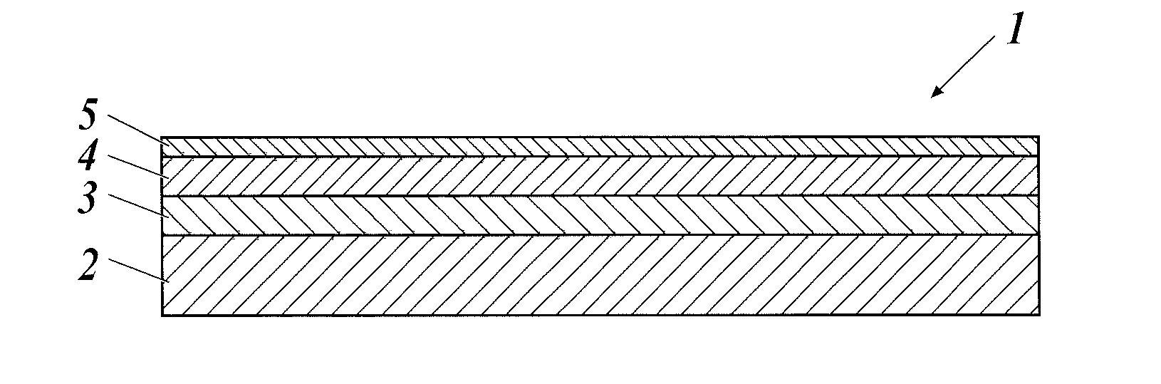
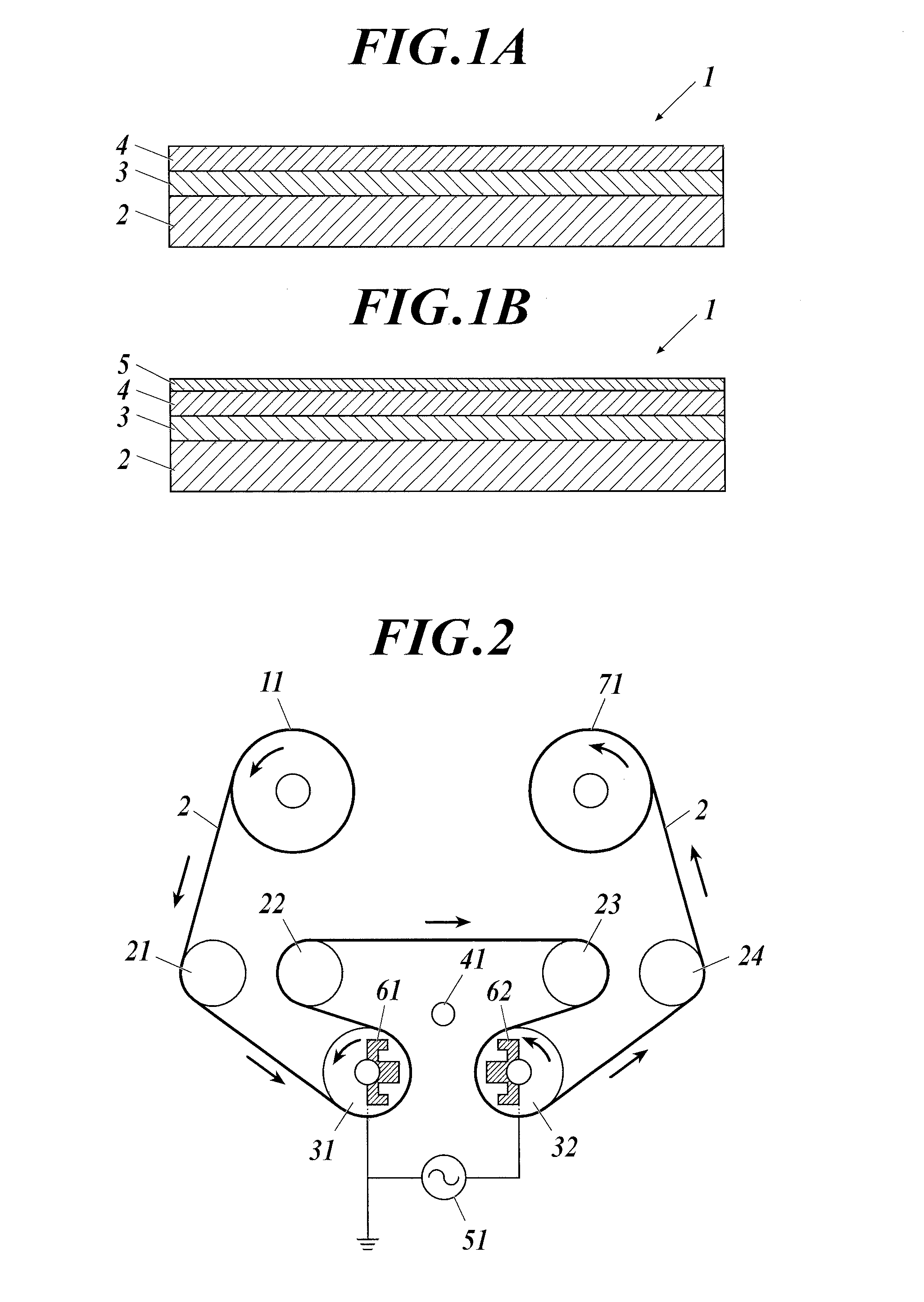
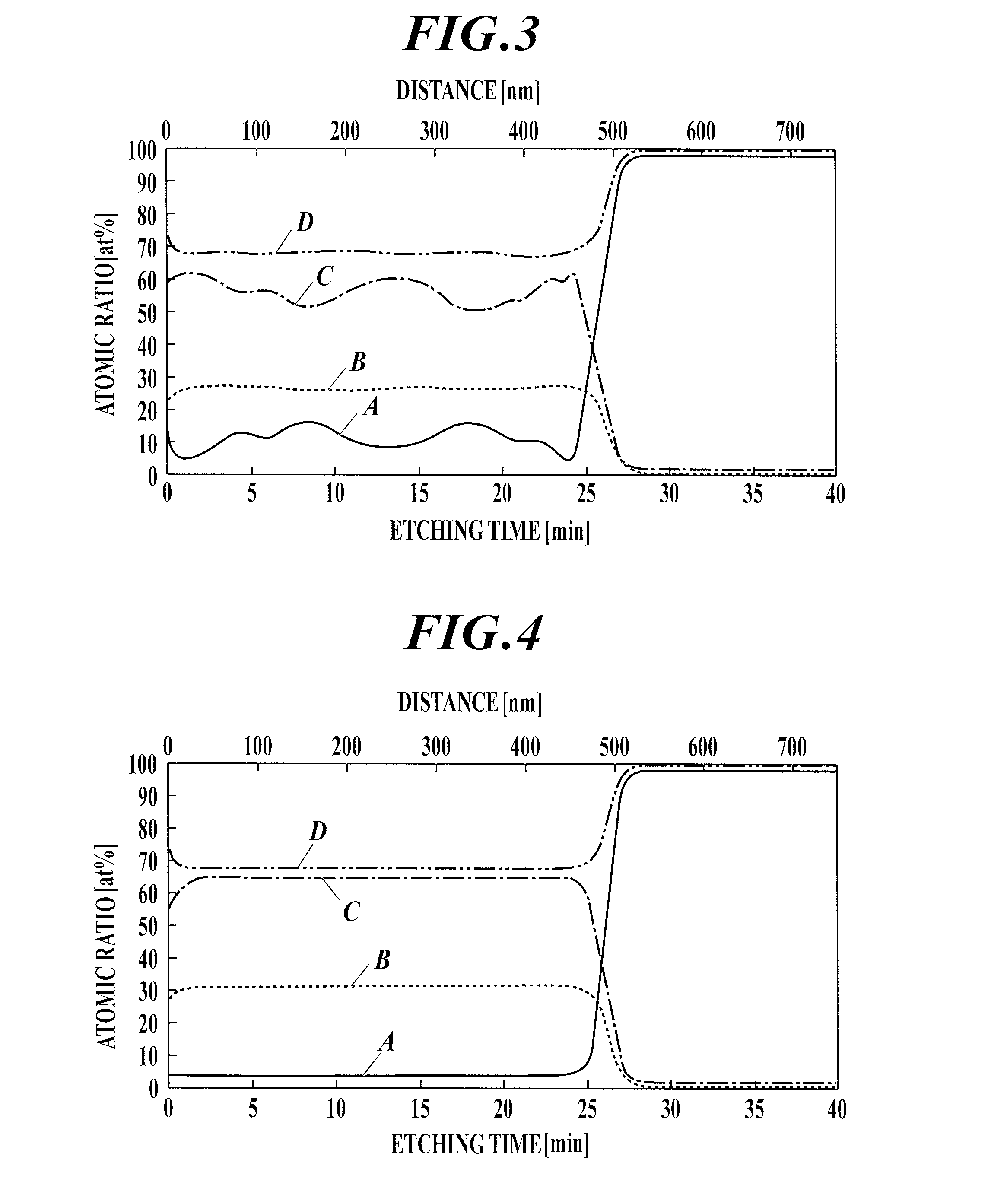
[0221]As a thermoplastic resin substrate (support), it was used a roll type polyester film treated with easy-adhesion processing on both surfaces and having a thickness of 125 μm (polyethylene terephthalate KDL86WA, made by Teijin-Dupont Co., Ltd., in the table, it is indicated as PET) without modification. A surface roughness (based on JIS B 0601) of the resin substrate was measured. It was found that an arithmetic average roughness Ra was 4 nm and ten points average roughness Rz was 320 nm.

>

[Preparation of Resin Substrate 1 Having a Smoothing Layer]

[0222]A coating liquid 1 for forming a smoothing layer as described below was coated on a surface side of the resin substrate placed with a gas barrier layer with a wire bar to make a dry thickness of 4 μm. Subsequently, the coated layer was dried at 80° C. for 3 minutes, then, it was cured with a high pressure mercury lamp under the curing condition of 0.5 J / cm2. Thus, Resin substrate having a smoothing la...

example 2

Preparation of Organic EL Element

[0350]By using gas barrier films 1 to 25 prepared in Example 1, organic EL elements 1 to 25 were prepared according to the following method as an example of an electronic device.

[Preparation of Organic EL Element 1]

(Formation of First Electrode Layer)

[0351]On the gas barrier film 1 prepared in Example 1, an ITO (indium tin oxide) film of 150 nm thickness was formed with a sputter method. Then, a first electrode layer was prepared by making pattering with photolithography. Here, the pattern was made so that the light emitting area became a 50 mm2.

(Formation of Hole Transport Layer)

[0352]On the first electrode layer provided with the gas barrier film 1 thus prepared was applied a coating liquid for forming a hole transport layer as described below under the conditions of 25° C. and relative humidity 50% with an extruding coater. Then, the coated layer was subjected to a drying treatment and a heating treatment to form a hole transport layer. Here, the ...


PUM

PropertyMeasurementUnit
surface free energyaaaaaaaaaa
wavelengthaaaaaaaaaa
RHaaaaaaaaaa

Abstract

A method for producing a gas barrier film includes forming a smoothing layer on one surface of a resin substrate; and forming a gas barrier layer containing a carbon atom, a silicon atom and an oxygen atom on a surface of the smoothing layer. The surface of the smoothing layer is controlled to have a dispersion component of a surface free energy in the range of 30 to 40 mN / m at an environment of 23° C. and 50% RH. The gas barrier layer is formed employing a raw material gas containing an organic silicon compound and an oxygen gas with a discharge plasma chemical vapor deposition method having a discharge space between rollers applied with a magnetic field.

Description

TECHNICAL FIELD[0001]The present invention relates generally to a gas barrier film and a method for producing the same, and an electronic device employing the same. More specifically, the present invention relates to a gas barrier film mainly used for an electronic device such as an organic electroluminescent element (hereafter, it is called as an organic EL element) and a method for producing the same, and an electronic device employing the same gas barrier film.BACKGROUND[0002]In the past, a gas barrier film, which is formed by laminating a plurality of layers containing a thin film of a metal oxide such as aluminum oxide, magnesium oxide, or silicon oxide on a surface of a plastic substrate or film, has been widely used for a package of an article required for blocking of a variety of gases such as water vapor and oxygen, for example, for a package application to prevent deterioration of foods, industrial products and medicines.[0003]A gas barrier film has been requested to be us...

Claims


Application Information

Patent Timeline
Patent Type & Authority Applications(United States)
IPC IPC(8): H01L51/52C23C16/48C23C16/50
CPCH01L51/5246C23C16/48C23C16/50C23C16/325C23C16/401C23C16/509C23C16/545H10K50/844H10K50/8426
Inventor EZURE, HIDETOSHI
Owner KONICA MINOLTA INC
Why Eureka
Try Eureka