Dynamic random access memory cell including a ferroelectric capacitor

a ferroelectric capacitor and random access technology, applied in capacitors, transistors, capacitors with voltage varied dielectrics, etc., can solve the problems of reducing the amount of charge stored by the electrodes, changing a stored logical value, and potentially falling below the retention time threshold. , to achieve the effect of reducing power consumption, reducing capacitor size, and reducing the size of the capacitor

Inactive Publication Date: 2016-03-03
QUALCOMM INC
View PDF15 Cites 45 Cited by
  • Summary
  • Abstract
  • Description
  • Claims
  • Application Information

AI Technical Summary

Benefits of technology

[0013]One advantage provided by at least one of the disclosed embodiments is a DRAM cell that includes a capacitor that does not lose a stored logical value due to leakage current. Because the logical value is represented by a polarization state of bi-stable asymmetric crystalline material in the ferroelectric layer instead of by a charge stored at the electrodes of the capacitor, leakage current may not cause the logical value to change (e.g., degrade). A size of the capacitor may be reduced as compared to other DRAM capacitors without causing a retention time to potentially fall below a retention time threshold because the retention time is not reduced due to the leakage current. Thus, the capacitor may be scaled to a semiconductor fabrication process with process nodes of 20 nm or less, and the capacitor may have reduced power consumption as compared to other DRAM capacitors. In this manner, a 1T1C DRAM cell formed using the capacitor may have decreased size and increased retention time as compared to other 1T1C DRAM cells. In a particular embodiment, the DRAM cell may include a selector instead of a transistor (e.g., the DRAM cell may be a 1S1C DRAM cell), which may enable the DRAM cell to be “stacked” (e.g., disposed) on or above other 1S1C DRAM cells. Forming multiple 1S1C DRAM cells in a stacked configuration may enable the 1S1C DRAM cells to be included in a memory device having a 3-D memory architecture, which may increase DRAM density of a memory device without increasing a horizontal area occupied by the memory device in a semiconductor die.

Problems solved by technology

When the capacitor is in the charged state, leakage current causes a discharge of the capacitor over time, thus potentially changing a stored logical value.
However, when the electrodes of the capacitor are decreased in size, the amount of charge stored by the electrodes decreases.
If the size of the capacitor becomes too small, the retention time may potentially fall below a retention time threshold.
Additionally, increasing density of a DRAM memory structure with a reduced size is difficult.
However, the deep trench formation processes of 1T1C cells may not be further scaled to reduced feature sizes due to area limitation associated with the capacitor.
For at least this reason, scaling the DRAM structure to semiconductor fabrication processes with smaller process windows while increasing DRAM density is difficult.

Method used


Image

  • Dynamic random access memory cell including a ferroelectric capacitor
  • Dynamic random access memory cell including a ferroelectric capacitor
  • Dynamic random access memory cell including a ferroelectric capacitor

Examples


first embodiment

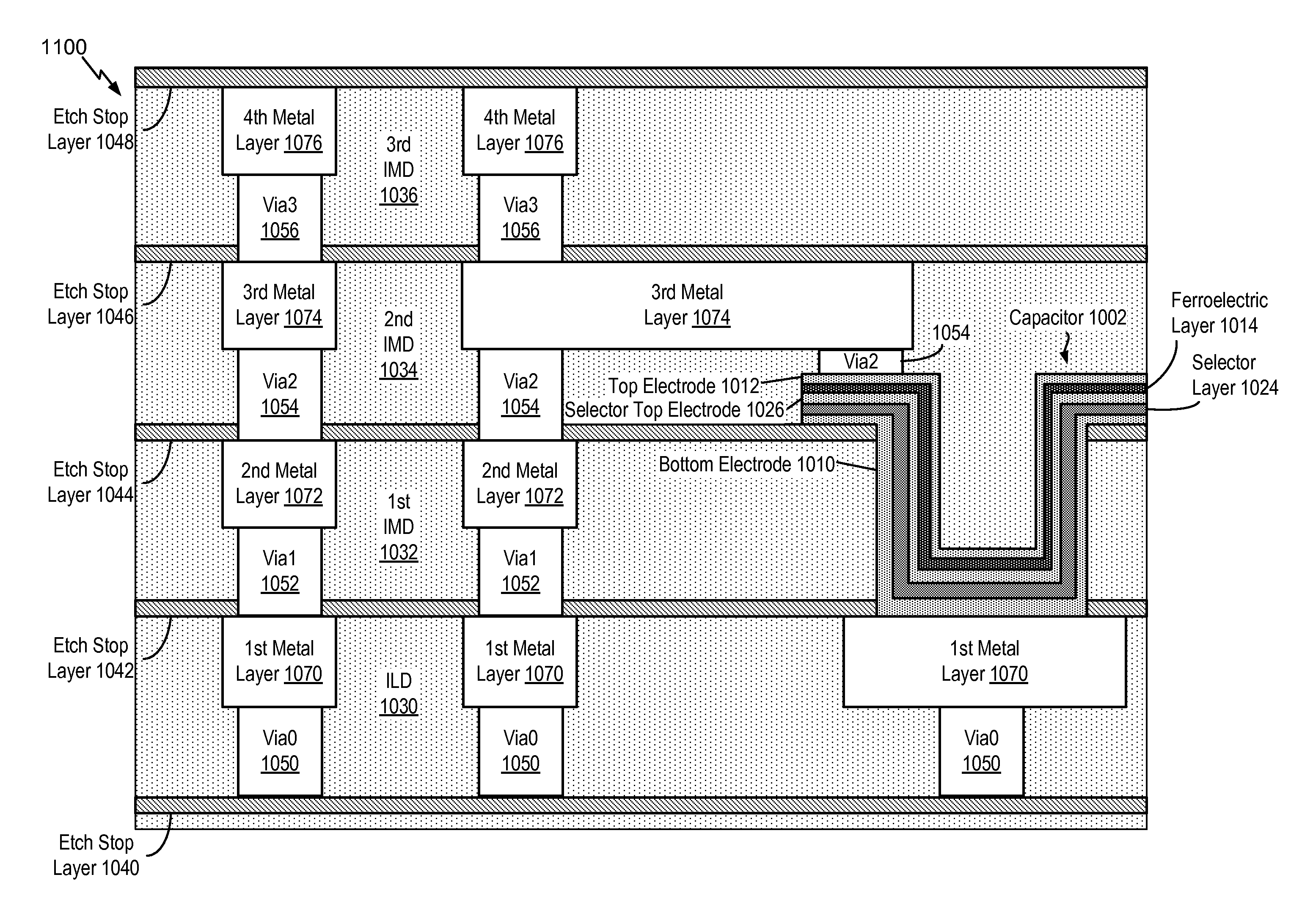
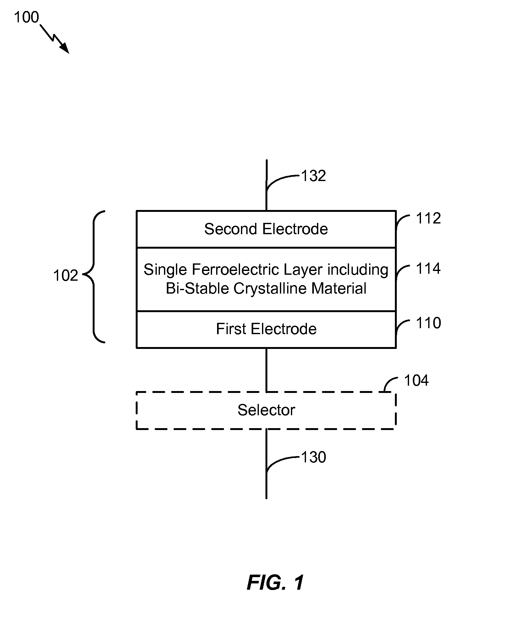
[0035]Referring to FIG. 1, a dynamic random-access memory (DRAM) cell 100 is shown. The DRAM cell 100 may include a capacitor 102 and a selector 104. In some embodiments, the selector 104 may be coupled in series with the capacitor 102, as further described with reference to FIGS. 2 and 3. In other embodiments, the selector 104 may be integrated within the capacitor 102, as further described with reference to FIGS. 4 and 5. In an alternate embodiment, the DRAM cell 100 may include a transistor coupled to the capacitor 102 instead of the selector 104. Multiple DRAM cells having a similar configuration to the DRAM cell 100 may be included in a memory array. In a particular embodiment, the multiple DRAM cells may be included in a cross-point DRAM array.

[0036]As shown in FIG. 1, the capacitor 102 may include a first electrode 110 (e.g., a bottom electrode), a second electrode 112 (e.g., a top electrode), and a single ferroelectric layer 114 disposed between the first electrode 110 and t...

second embodiment

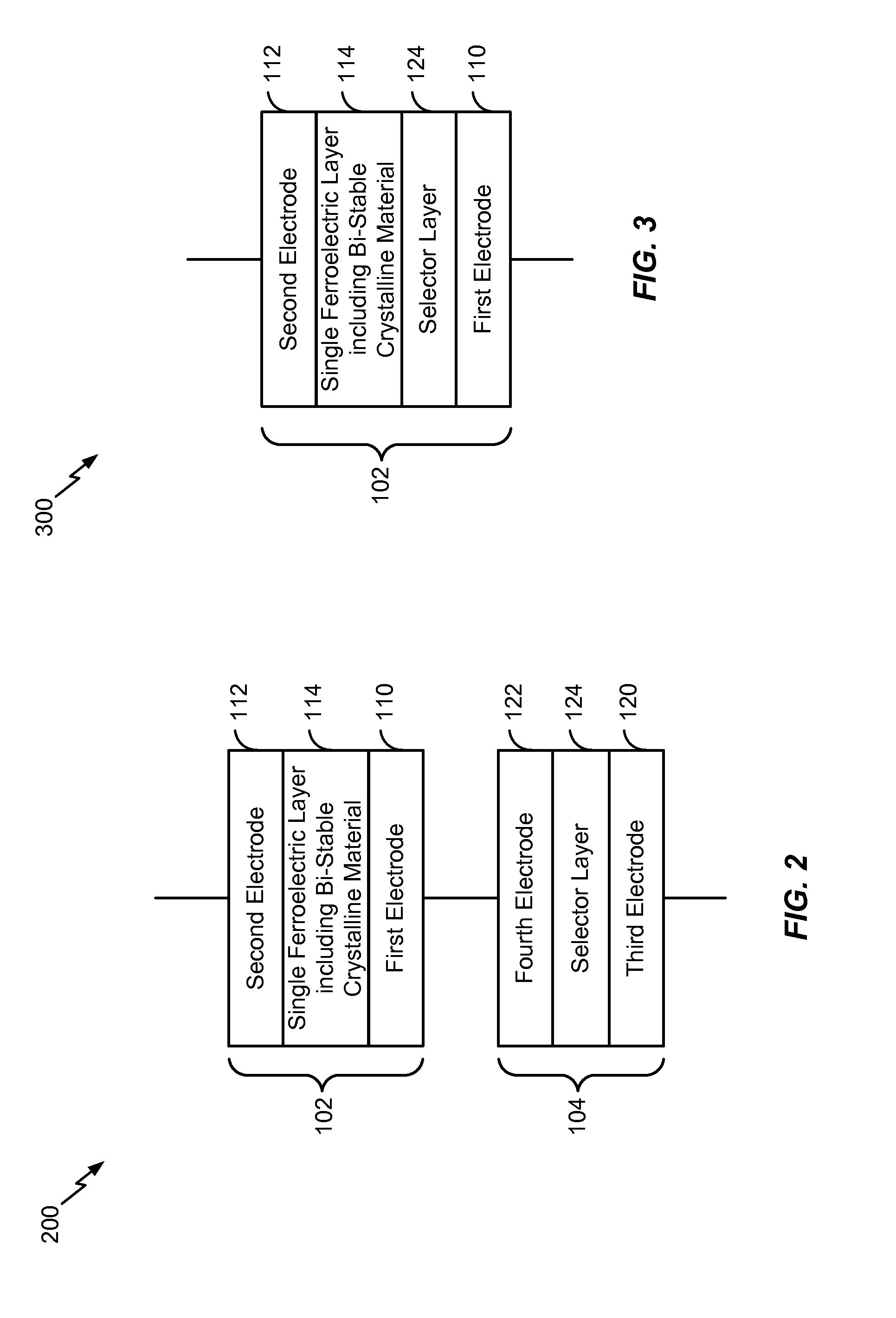
[0052]Referring to FIG. 2, the DRAM cell of FIG. 1 is shown and designated 200. In the DRAM cell 200, the selector 104 is separate from (e.g., external to) the capacitor 102 and is coupled in series with the capacitor 102. The capacitor 102 is configured as described with reference to FIG. 1.

[0053]As illustrated in FIG. 2, the selector 104 may include a third electrode 120 (e.g., a selector bottom electrode), a fourth electrode 122 (e.g., a selector top electrode), and a selector layer 124 disposed between the third electrode 120 and the fourth electrode 122. The selector layer 124 may include a voltage-dependant resistor layer. As described with reference to FIG. 1, the selector layer 124 may function in a similar manner to a diode. The selector layer 124 (e.g., the voltage-dependent resistor layer) may be formed as a film layer and may correspond to an insulator at low voltages. In a particular embodiment, the insulating film may include platinum (Pt), tantalum oxide (TaOx), titan...

third embodiment

[0055]Referring to FIG. 3, the DRAM cell of FIG. 1 is shown and designated 300. In the DRAM cell 300, the selector 104 is integrated within the capacitor 102. The capacitor 102 is configured as described with reference to FIG. 1.

[0056]As illustrated in FIG. 3, the selector layer 124 may be disposed between the single ferroelectric layer 114 and the first electrode 110. In a particular embodiment, the selector layer 124 may be in contact with the single ferroelectric layer 114. In an alternate embodiment, an electrode (e.g., a selector top electrode) may be disposed between the selector layer 124 and the single ferroelectric layer 114.

[0057]The selector layer 124 may include a voltage-dependant resistor layer. As described with reference to FIG. 1, the selector layer 124 may exhibit diode-type (e.g., non-linear) I-V characteristics (in a forward bias conditions). The selector layer 124 (e.g., the voltage-dependent resistor layer) may be formed as a film layer and may correspond to an...


PUM

PropertyMeasurementUnit
feature sizesaaaaaaaaaa
thicknessaaaaaaaaaa
thicknessaaaaaaaaaa

Abstract

A memory cell includes a capacitor that includes a first metal layer and a second metal layer. The capacitor includes a ferroelectric layer disposed between the first metal layer and the second metal layer. The ferroelectric layer is a single layer of a bi-stable asymmetric crystalline material.

Description

I. FIELD[0001]The present disclosure is generally related to a dynamic random access memory (DRAM) cell that includes a ferroelectric capacitor.II. DESCRIPTION OF RELATED ART[0002]Advances in technology have resulted in smaller and more powerful computing devices. For example, there currently exist a variety of portable personal computing devices, including wireless computing devices, such as portable wireless telephones, personal digital assistants (PDAs), and paging devices that are small, lightweight, and easily carried by users. More specifically, portable wireless telephones, such as cellular telephones and Internet protocol (IP) telephones, can communicate voice and data packets over wireless networks. Further, many such wireless telephones include other types of devices that are incorporated therein. For example, a wireless telephone can also include a digital still camera, a digital video camera, a digital recorder, and an audio file player. Also, such wireless telephones ca...

Claims


Application Information

Patent Timeline
Patent Type & Authority Applications(United States)
IPC IPC(8): H01L27/115G11C11/22G11C11/409H01L27/108
CPCH01L27/11507H01L27/10897H01L27/11514H01L27/11512G11C11/2275G11C11/409G11C11/221G11C11/2273H01L27/10805G11C11/401H01L28/40H01G7/06H01L28/91H10B12/31H10B53/30H10B12/30H10B12/50H10B53/20H10B53/50
Inventor LI, XIAKANG, WOO, TAGYUN, CHANGHAN, HOBIECHEN, WEI-CHUAN
Owner QUALCOMM INC
Why Eureka
Try Eureka