
Eureka
For R&D, Eureka makes reading and utilizing patents & technical documents easy.
Eureka AIR
Designed for self-driven R&D workflows. Generate viable solutions, solve complex R&D challenges, empower your innovation with AI.

Eureka Materials
Designed for material experts only. Revolutionize your material R&D, from search, analyze, to developing new materials.

TechResearch
Generate reliable direction feasibility study reports for your R&D in just a few steps.

TechSeek
Discover and master advanced knowledge NOW. Basics, ideas, possibilities, all at once.

TechMind
As an expert in R&D Theories, TechMind can generates customized viable solutions instantly.

TechRisk
Analyze your overall solution with one click, know your potential R&D risks in advance.

TechMonitor
Get weekly tech updates, stay abreast of the latest tech innovations and key insights.
Light-absorbing layer and layer system containing the layer, method for producing the layer system and a sputter target suited therefor
- Summary
- Abstract
- Description
- Claims
- Application Information
AI Technical Summary
Benefits of technology
Problems solved by technology
Method used
Image

Examples
example 2
Layer Systems of Conductor Path and Absorber Layer
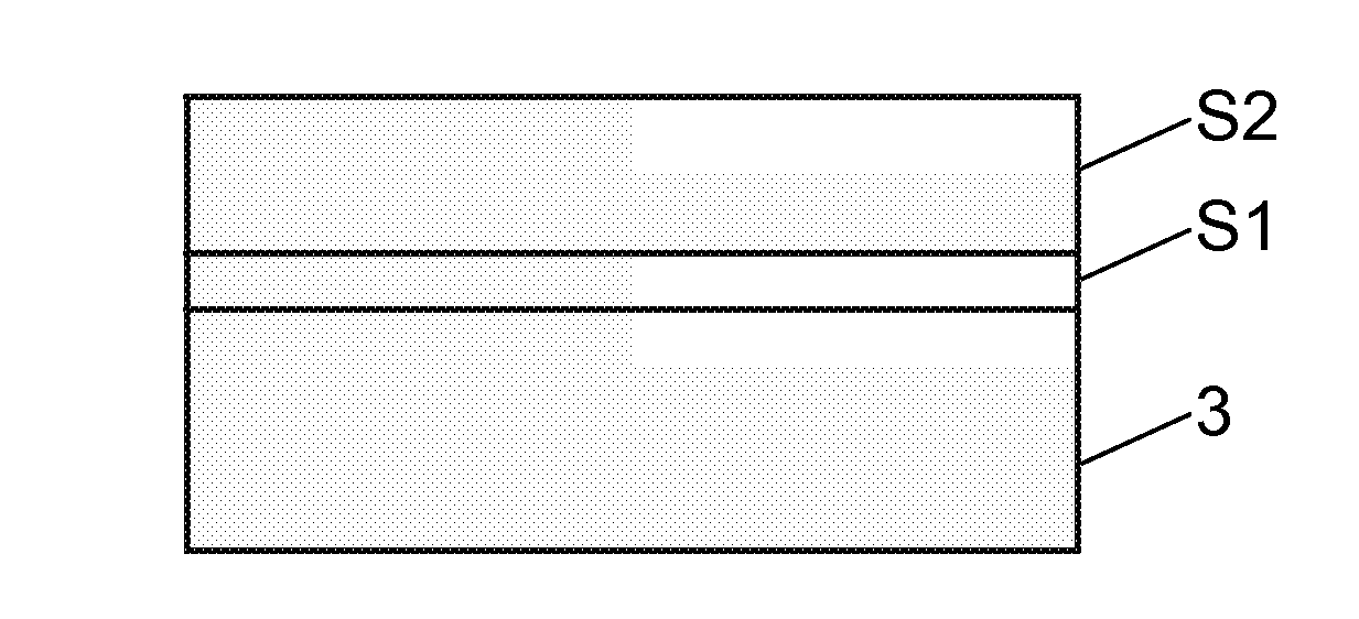
[0156]A further layer system according to the invention refers to “black conductor paths”. These consist of a thin base layer of Al, Cu, Mo or Ti or of alloys of said metals that have an almost black appearance due to a coating of substoichiometric zinc-molybdenum oxide with suitably selected layer thickness and thus show a high electrical conductivity.
[0157]The following properties can be achieved with such a layer system:
Tv<8%, preferably <4%
Rv<15%
[0158]layer resistance <100Ω / square
simple wet etching, e.g. with diluted acids based on HNO3, HCl, oxalic acid, acetic acid, phosphoric acid (also mixtures of said acids) or fluoride-containing compounds such as NH4HF2
small layer thickness <100 nm, preferably <60 nm.
[0159]The layer sequence is here: substrate / metal / black absorber layer. In an alternative embodiment of the layer system according to the invention, the layer sequence is inverse, namely: glass substrate / black absorber layer...
example 5
Single-Layered Black Absorber Layer
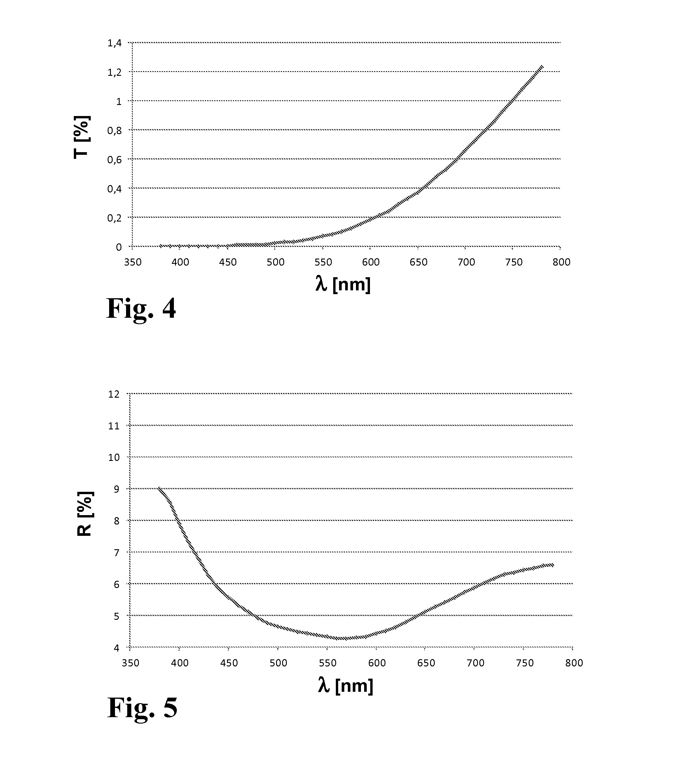
[0196]A single-layered absorber layer S2 (without antireflection layer S1) deposited on a glass substrate, with the chemical composition of Sample 1 of Table 1, turns out to be visually opaque and black. FIGS. 12 and 13 show the curve of the reflection R (in %) and the transmission T (in %) over the wavelength range λ (in nm) of 350 nm to 750 nm. The dark gray curve L1 must here be assigned to a thin single-layered absorber layer with a mean layer thickness of 125 nm, and the light gray curve L2 to a single-layered absorber layer with a mean thickness of 145 nm.
[0197]The visual reflection of the thinner absorber layer L1 is 8.9% and that of the thicker absorber layer L2 is 10%. The reflection measured on the bottom side of the glass substrate remains below 12% over the whole wavelength range. In the range of the wavelengths that correspond to the maximum eye sensitivity in daylight (around 550 nm), the reflections values are even around 10% or belo...
PUM
| Property | Measurement | Unit |
|---|---|---|
| Fraction | aaaaa | aaaaa |
| Fraction | aaaaa | aaaaa |
| Fraction | aaaaa | aaaaa |
Abstract
Description
Claims
Application Information
 - R&D Engineer
- R&D Manager
- IP Professional
- Industry Leading Data Capabilities
- Powerful AI technology
- Patent DNA Extraction
Browse by: Latest US Patents, China's latest patents, Technical Efficacy Thesaurus, Application Domain, Technology Topic, Popular Technical Reports.
© 2024 PatSnap. All rights reserved.Legal|Privacy policy|Modern Slavery Act Transparency Statement|Sitemap|About US| Contact US: help@patsnap.com