Method for semiconductor selective etching and bsi image sensor
- Summary
- Abstract
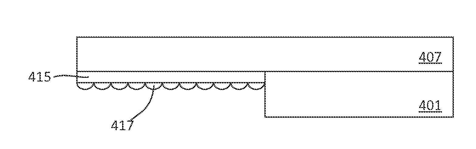
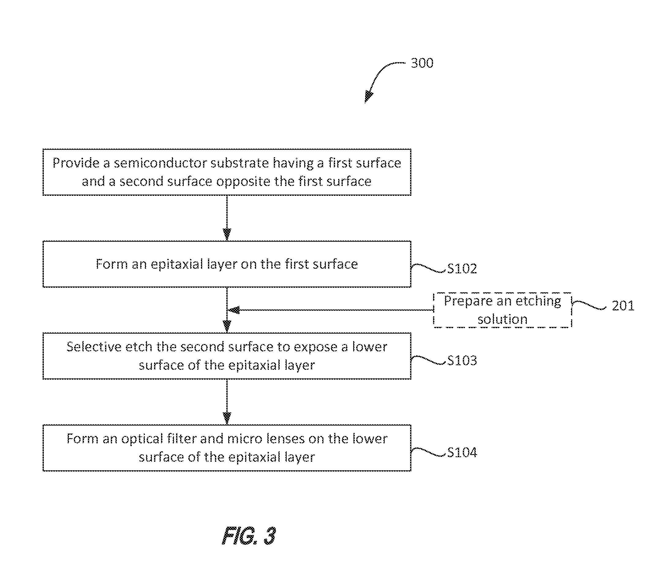
- Description
- Claims
- Application Information
AI Technical Summary
Benefits of technology
Problems solved by technology
Method used
Image

Examples
example 1
[0042]1. Etching Solution Preparation
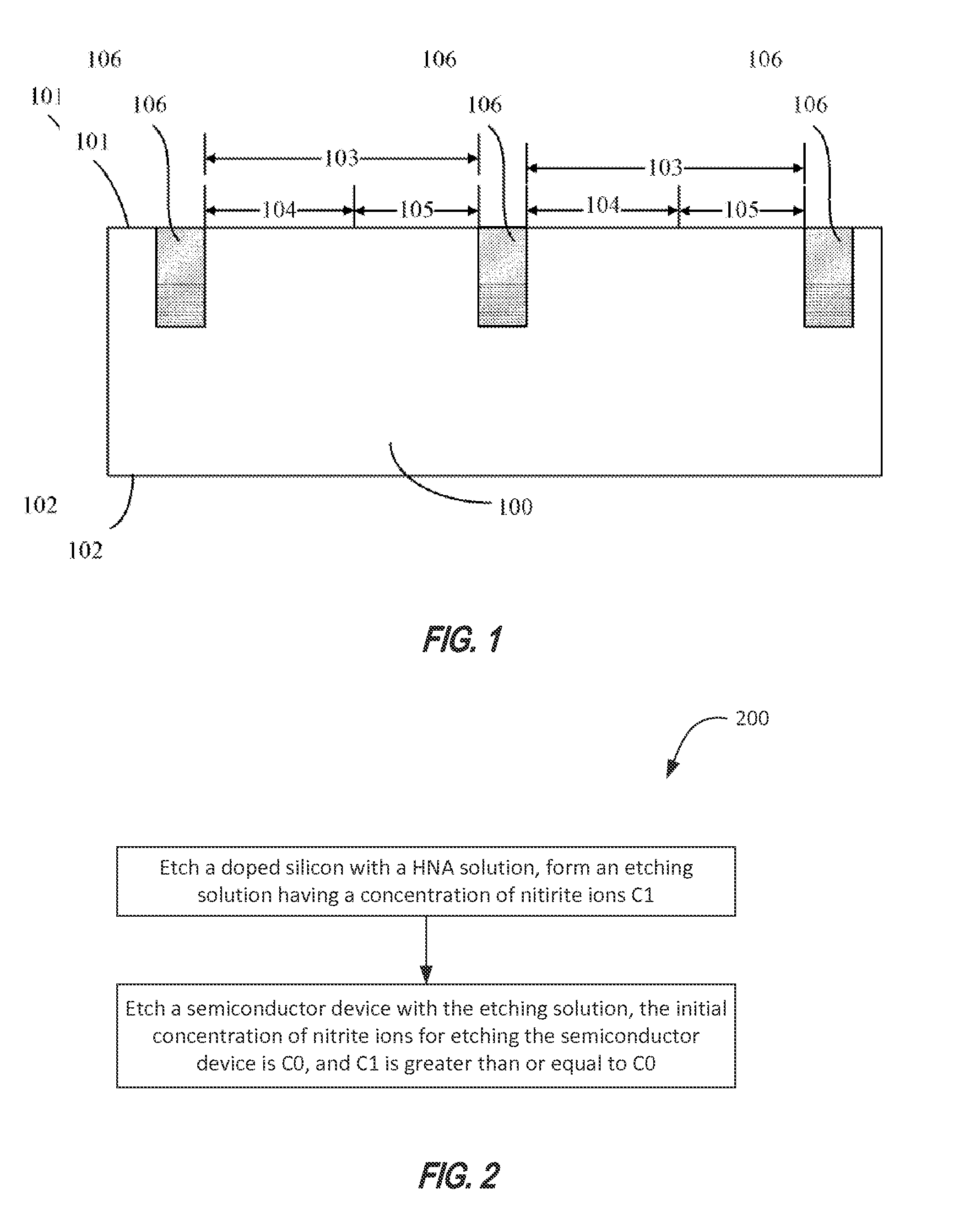
[0043]A P-type silicon substrate is provided. The silicon substrate has a resistivity in the range of 0.006 to 0.01 Ω·cm and is doped with a doping concentration higher than 1×10¹⁸ atoms / cm3. The silicon substrate is then submitted to marking, cleaning, back-grinding, flipping, chemical mechanical polishing, and the like. An HNA solution is sprayed onto the silicon substrate and evenly distributed on the surface of the silicon substrate through a low rotation speed (3, and CH3COOH in a volume ratio of 1:3:8, the mass concentration percentage of HF is 49%, the mass concentration percentage of HNO3 is 70%, and the mass concentration percentage of CH3COOH is 100%.
[0044]During the rotation, the proportion of HNO2 in the HNA solution gradually increases. The etching process stops when the etch rate reaches a stable value, and an etching solution is obtained from the HNA solution. A process for determining the etch rate can include measuring the thickn...
example 2
[0054]1. Etching Solution Preparation
[0055]A P-type silicon substrate is provided. The silicon substrate has a resistivity in the range of 0.01 to 0.02 Ω·cm and is doped with a doping concentration higher than 1×10¹⁷ atoms / cm3. The silicon substrate is then submitted to marking, cleaning, back-grinding, flipping, chemical mechanical polishing, and the like. An HNA solution is sprayed onto the silicon substrate and evenly distributed on the surface of the silicon substrate through a low rotation speed (3, and CH3COOH in a volume ratio of 5:1:4, the mass concentration percentage of HF is 49%, the mass concentration percentage of HNO3 is 70%, and the mass concentration percentage of CH3COOH is 100%. The etch rate can be determined using the same processes as described in Example 1 above and are denoted S3.
[0056]2. Testing the Etch Rate of the Etching Solution
[0057]The etch rates of the etching solution are measured using the same P-type silicon substrates. The P-type silicon substrates...
example 3
[0066]1. Etching Solution Preparation
[0067]An N-type silicon substrate is provided. The N-type silicon substrate has a resistivity in the range of 0.05 to 0.08 Ω·cm and is doped with a doping concentration higher than 1×10¹⁶ atoms / cm3. The N-type silicon substrate is then submitted to marking, cleaning, back-grinding, flipping, chemical mechanical polishing, and the like. An HNA solution is sprayed onto the silicon substrate and evenly distributed on the surface of the silicon substrate through a low rotation speed (3, and CH3COOH in a volume ratio of 3:5:2, the mass concentration percentage of HF is 30%, the mass concentration percentage of HNO3 is 60%, and the mass concentration percentage of CH3COOH is 80%. The etch rate can be determined using the same processes as described in Example 1 above and are denoted S5.
[0068]2. Testing the Etch Rate of the Etching Solution
[0069]The etch rates of the etching solution are measured using same N-type silicon substrates. The N-type silicon ...
PUM
 Abstract
Description
Claims
Application Information
 - R&D
- Intellectual Property
- Life Sciences
- Materials
- Tech Scout
- Unparalleled Data Quality
- Higher Quality Content
- 60% Fewer Hallucinations
Browse by: Latest US Patents, China's latest patents, Technical Efficacy Thesaurus, Application Domain, Technology Topic, Popular Technical Reports.
© 2025 PatSnap. All rights reserved.Legal|Privacy policy|Modern Slavery Act Transparency Statement|Sitemap|About US| Contact US: help@patsnap.com