
Silicon carbide semiconductor device and manufacturing method of the same

a technology of silicon carbide and semiconductor devices, which is applied in the direction of semiconductor devices, electrical devices, transistors, etc., can solve the problems of further reduction of resistance, low solid-solubility limit, and insufficient characteristics

Active Publication Date: 2016-05-19
HITACHI LTD
View PDF1 Cites 15 Cited by
  • Summary
  • Abstract
  • Description
  • Claims
  • Application Information

AI Technical Summary

Benefits of technology

The patent describes a method for manufacturing a silicon carbide semiconductor device that can provide high performance and reliability. The method involves a combination of steps, including forming an epitaxial layer and drain region, creating a mask to implant impurities, and using a sidewall mask to create a second source region. This method can be used even when nitrogen or other difficult-to-diffuse impurities are used in the source diffusion layer of a contact portion. Overall, this method allows for the fabrication of high-quality silicon carbide semiconductor devices with reliable performance.

Problems solved by technology

However, considering the original characteristics to be obtained from silicon carbide (SiC), it cannot be said that sufficient characteristics have been obtained, and further reduction of the ON resistance has been desired from the viewpoint of high efficient utilization of energy.
One of the problems to be solved for the ON resistance of the SiC power MISFET of a DMOS (Double diffused Metal Oxide Semiconductor) structure is a parasitic contact resistance on a contact surface between a source diffusion layer and a metal electrode, which is a unique problem in the SiC power MISFET.
In the case where the nitrogen is used as an impurity, there is a problem in that a solid-solubility limit is low and electrical activation is not sufficiently achieved even when the impurity is implanted at a high concentration.

Method used


Image

  • Silicon carbide semiconductor device and manufacturing method of the same
  • Silicon carbide semiconductor device and manufacturing method of the same
  • Silicon carbide semiconductor device and manufacturing method of the same

Examples


first embodiment

[0049]>

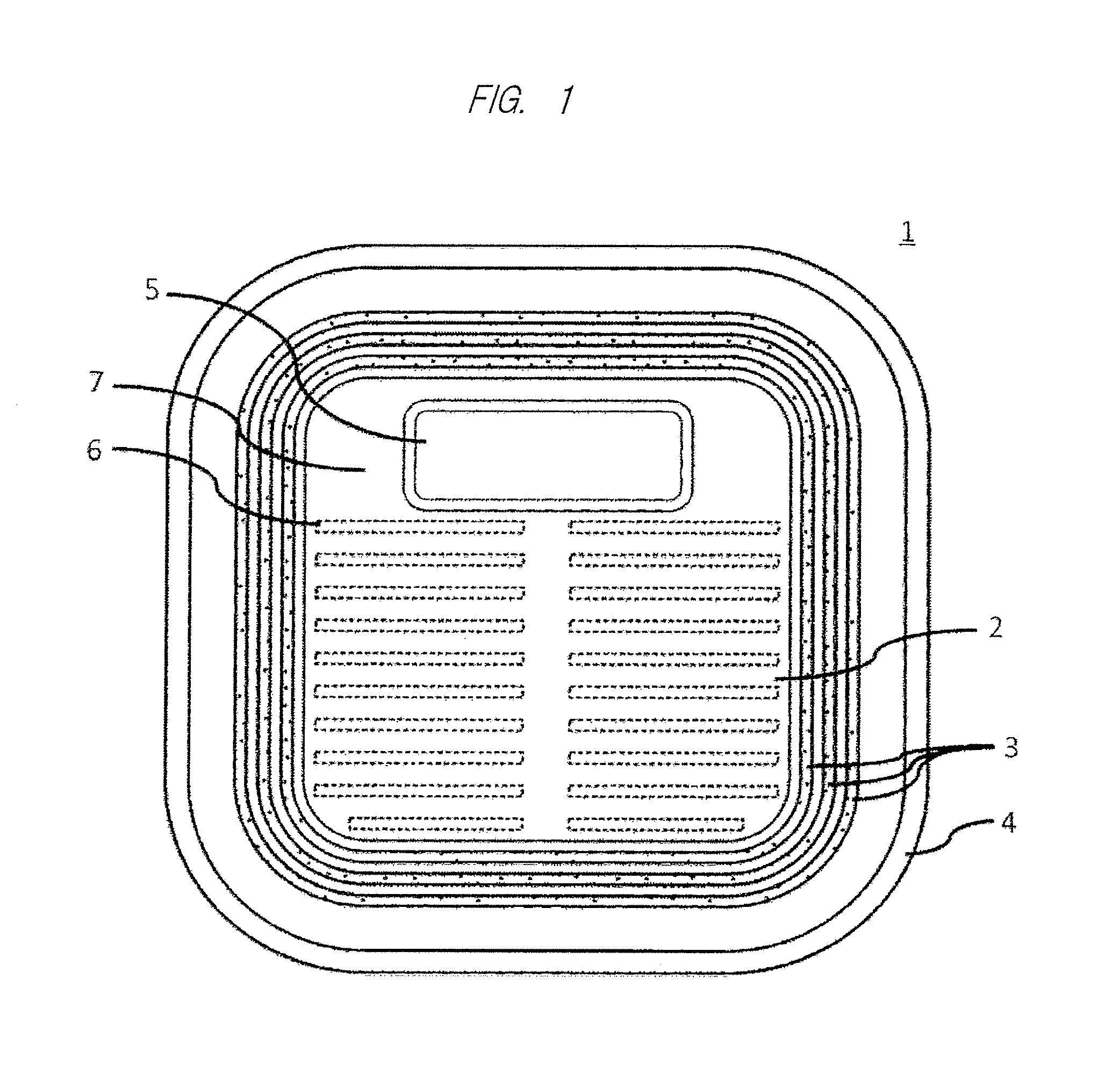
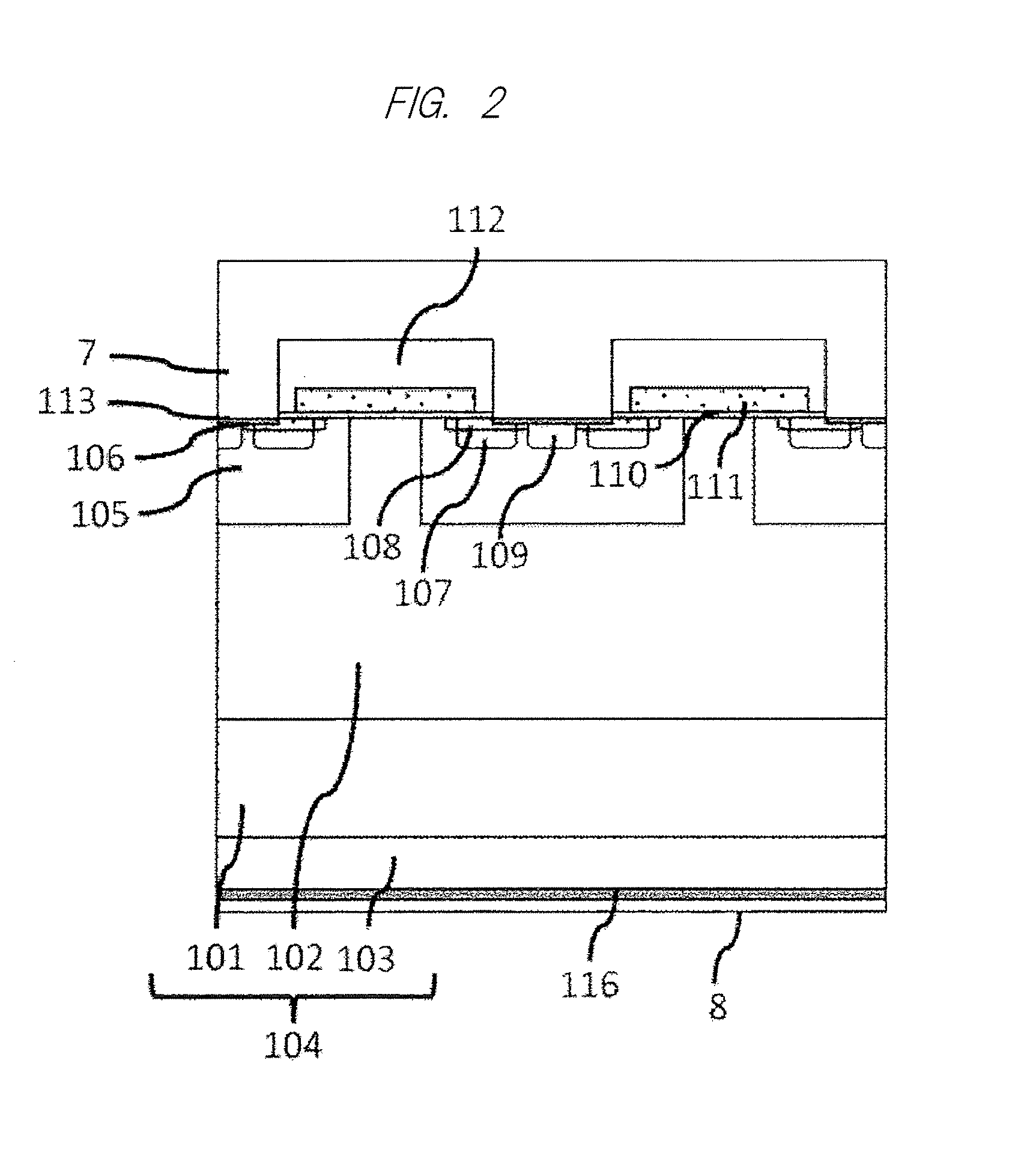
[0050]A structure of the silicon carbide semiconductor device according to the first embodiment of the present invention will be described with reference to FIGS. 1 and 2. FIG. 1 is a top view illustrating a principal part of a semiconductor chip in which the silicon carbide semiconductor device constituted of a plurality of SiC power MISFETs is mounted, and FIG. 2 is a cross-sectional view illustrating a principal part of the SiC power MISFET. The SiC power MISFET constituting the silicon carbide semiconductor device is a MISFET of a DMOS structure.

[0051]As illustrated in FIG. 1, a semiconductor chip 1 in which the silicon carbide semiconductor device is mounted includes an active region (an SiC power MISFET forming region, an element forming region) 2 in which a plurality of n-channel SiC power MISFETs are connected in parallel and a peripheral forming region surrounding the active region 2 when seen in a plan view. In the peripheral forming region, a plurality of p-type fl...

second embodiment

[0101]A difference between the second embodiment and the above-mentioned first embodiment lies in a method of forming the source region. Namely, in the second embodiment, an n++-type second source region 208 is made shallower than an n+-type first source region 206 as illustrated in FIG. 17, and thus the second source region 208 becomes equivalent to the third source region. Note that the reference numeral 201 indicates an n+-type SiC substrate (substrate), the reference numeral 202 indicates an n−-type epitaxial layer, the reference numeral 203 indicates an n+-type drain region, the reference numeral 204 indicates an SiC epitaxial substrate, the reference numeral 205 indicates a p-type body layer (well region), the reference numeral 209 indicates a p+-type body layer potential fixing region, the reference numeral 210 indicates a gate insulating film, the reference numeral 211 indicates a gate electrode, the reference numeral 212 indicates an interlayer insulating film, the referenc...

third embodiment

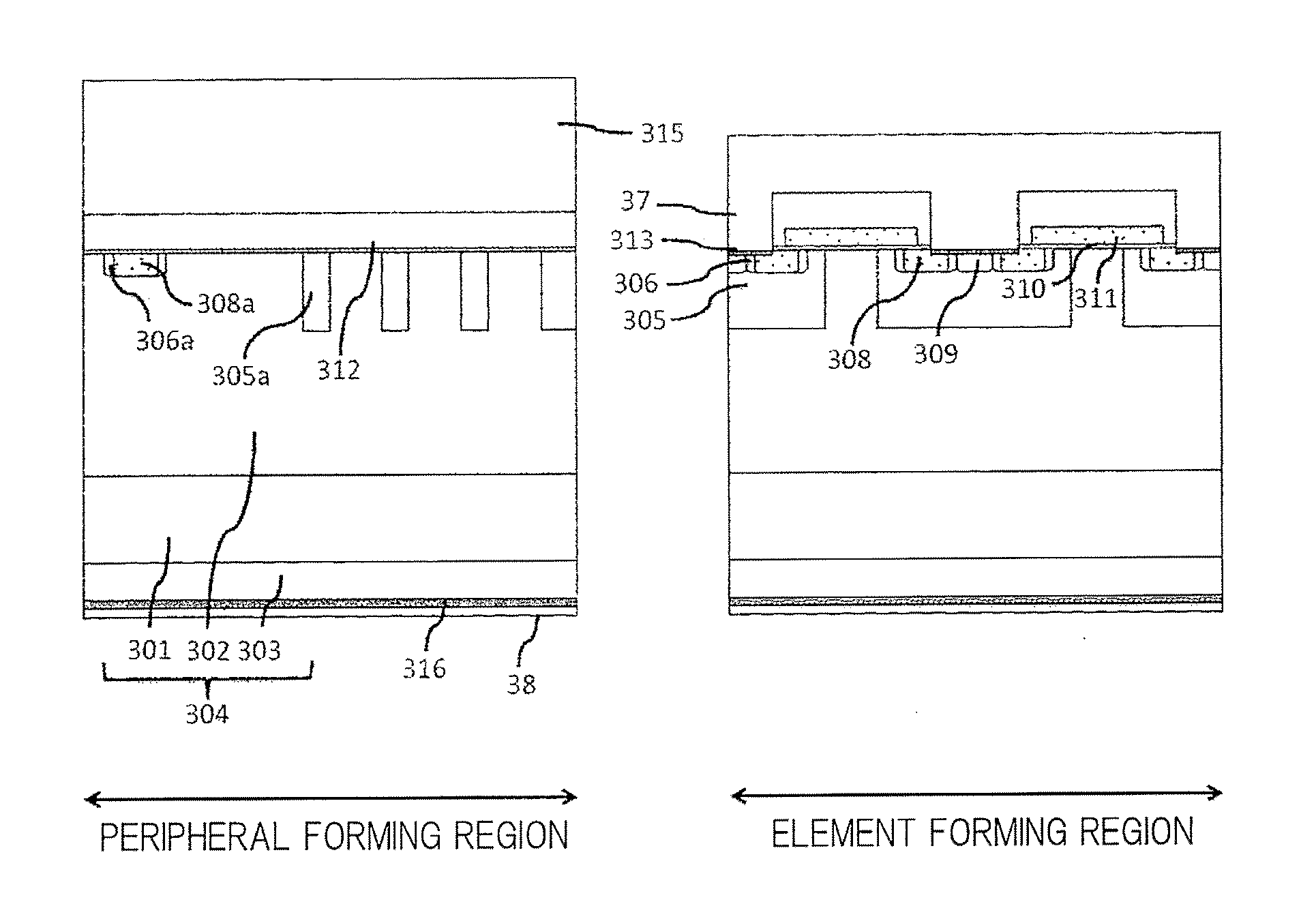
[0114]A difference between the third embodiment and the above-mentioned first and second embodiments lies in a method of forming the source region. Namely, in the third embodiment, the depth of an n++-type second source region 308 is made equal to the depth of an n+-type first source region 306 as illustrated in FIG. 22. Note that the reference numeral 301 indicates an n+-type SiC substrate (substrate), the reference numeral 302 indicates an n−-type epitaxial layer, the reference numeral 303 indicates an n+-type drain region, the reference numeral 304 indicates an SiC epitaxial substrate, the reference numeral 305 indicates a p-type body layer (well region), the reference numeral 309 indicates a p+-type body layer potential fixing region, the reference numeral 310 indicates a gate insulating film, the reference numeral 311 indicates a gate electrode, the reference numeral 312 indicates an interlayer insulating film, the reference numeral 313 indicates a metal silicide layer, the ref...


PUM


Abstract

In order to provide a high-performance and reliable silicon carbide semiconductor device, in a silicon carbide semiconductor device including an n-type SiC epitaxial substrate, a p-type body layer, a p-type body layer potential fixing region and a nitrogen-introduced n-type first source region formed in the p-type body layer, an n-type second source region to which phosphorus which has a solid-solubility limit higher than that of nitrogen and is easily diffused is introduced is formed inside the nitrogen-introduced n-type first source region so as to be separated from both of the p-type body layer and the p-type body layer potential fixing region.

Description

TECHNICAL FIELD[0001]The present invention relates to a silicon carbide semiconductor device which is constituted of a plurality of power semiconductor devices using a silicon carbide substrate, and a manufacturing method of the same.BACKGROUND ART[0002]Conventionally, in a power metal insulator semiconductor field effect transistor (MISFET) which is one of the power semiconductor devices, a power MISFET using a silicon (Si) substrate (hereinafter, referred to as an Si power MISFET) has been a mainstream.[0003]However, the power MISFET using a silicon carbide (SiC) substrate (hereinafter, referred to as an SiC substrate) (hereinafter, referred to as an SiC power MISFET) can achieve higher breakdown voltage and lower loss compared to the Si power MISFET. Therefore, the SiC power MISFET has drawn attention in the field of power saving or eco-friendly inverter technologies.[0004]Compared to the Si power MISFET, the SiC power MISFET can achieve a lower ON resistance at the same breakdow...

Claims


Application Information

Patent Timeline
IPC IPC(8): H01L29/16H01L29/08H01L29/06H01L29/66H01L21/04H01L21/02H01L29/78H01L29/167H01L29/10
CPCH01L29/1608H01L29/167H01L29/086H01L29/0865H01L29/0878H01L29/0882H01L29/66068H01L29/1095H01L21/0465H01L21/02378H01L21/02529H01L29/7802H01L29/0619H01L21/0485H01L29/0869H01L29/78H01L29/7811
Inventor TEGA, NAOKIKOBAYASHI, KEISUKEFUJISAKI, KOJITAKAHAMA, TAKASHI
Owner HITACHI LTD
Learn More