Catalysts for Carbon Dioxide Conversion
a carbon dioxide and catalyst technology, applied in the direction of physical/chemical process catalysts, electrochemical coatings, organic compounds/hydrides/coordination complex catalysts, etc., to achieve the effect of improving co2 reduction, increasing conversion performance, and reducing costs
- Summary
- Abstract
- Description
- Claims
- Application Information
AI Technical Summary
Benefits of technology
Problems solved by technology
Method used
Image
Examples
example 1
MoS2 Characterization
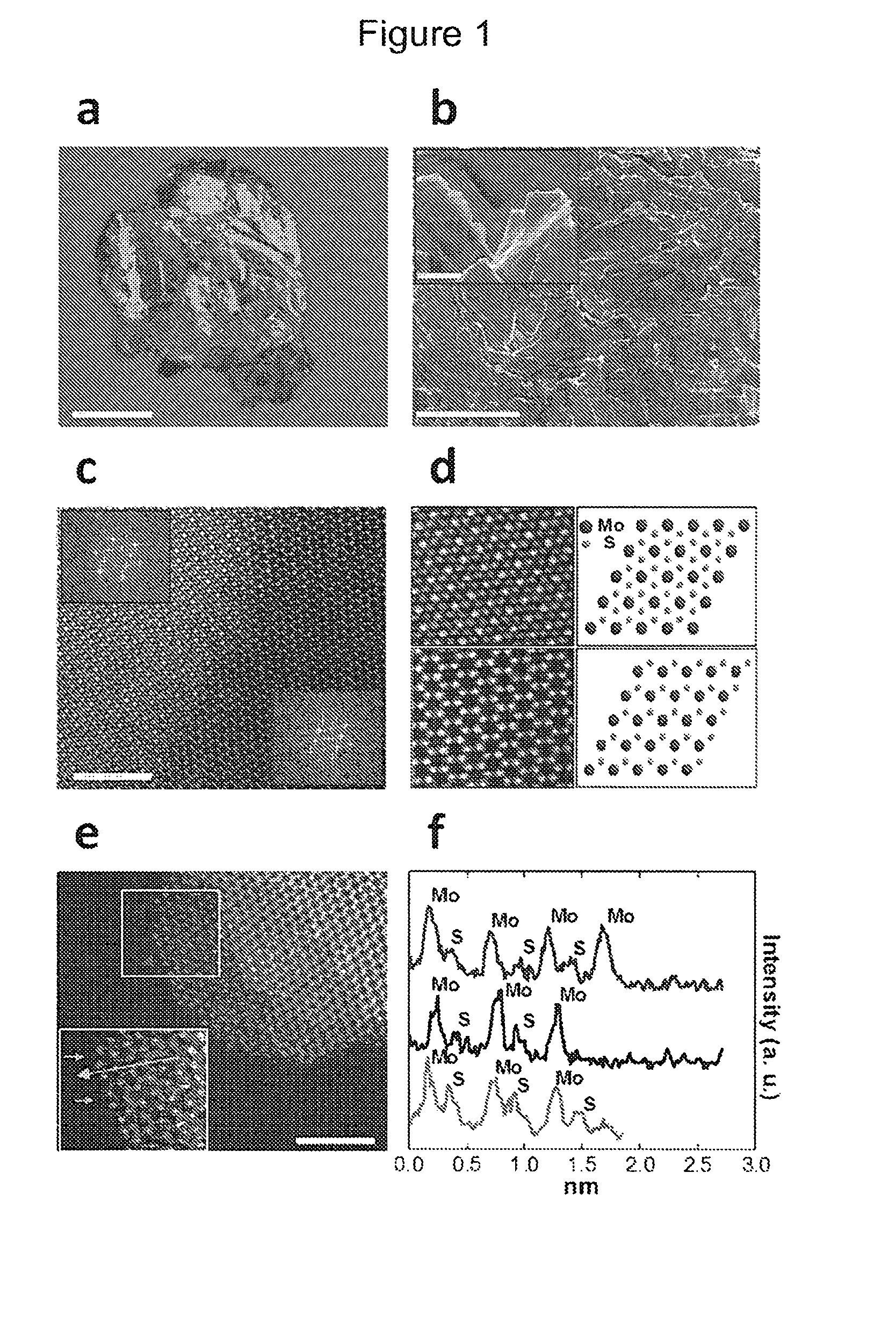
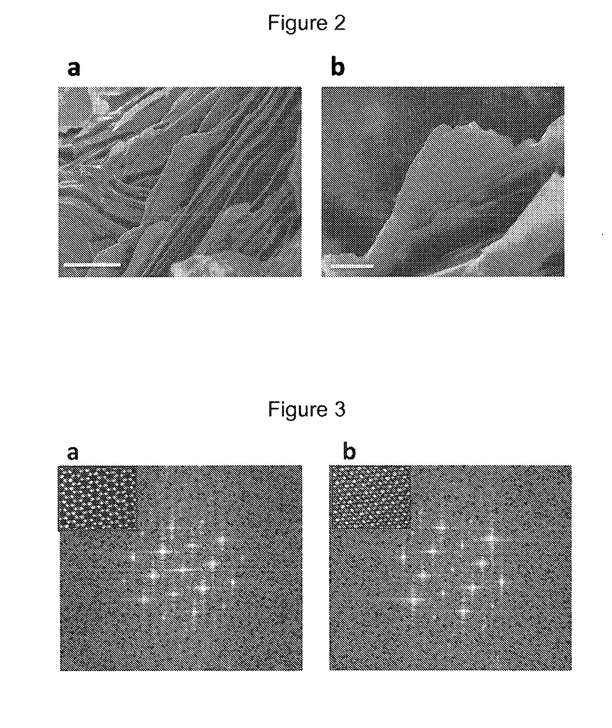
[0074]Morphology of MoS2 was visualized at different scales. Optical characterizations were performed by using a Stereo-F (16×-100× microscope) at 2× magnification and digital images of bulk MoS2 (purchased through SPI Supplies) were taken using a 5 mega pixels (MP) CCD camera mounted on the microscope. Scanning Electron Microscopy (SEM) was performed in order to characterize the morphology of the bulk MoS2 at micro scale. The instrument used for characterization is integrated in a Raith e-LiNE plus ultra-high resolution electron beam lithography system. During imaging the samples were kept at a distance of 10 mm from the electrons source and the voltage was kept at 10 kV. No particular types of preparation were implemented before imaging. To visualize atomic structure, scanning transmission electron microscopy (STEM) was performed using a probe-corrected JEOL JEM-ARM200CF equipped with a 200 kV cold-field emission gun (CFEG). Images were acquired in either the ...
example 2
[0075]Raman spectroscopy (Renishaw Raman 2000) was used to detect the MoS2 in-plane and out of plane phonon mode. The spectrum was obtained by exposing small pieces of the samples i.e. bulk MoS2 (without any particular treatment) to 514 nm laser beam (Ar laser, power 10 mW and spot size 10 μm).
example 3
Ultraviolet Photoelectron Spectroscopy (UPS)
[0076]Surface work function measurements were carried out using ultraviolet photoelectron spectroscopy (UPS). UPS data were acquired with a Physical Electronics PHI 5400 photoelectron spectrometer using Hel (21.2 eV) ultraviolet radiation and a pass energy of 8.95 eV. To separate the signal arising from secondary electron emission from the detector from the secondary electron emission from the sample, a −9 V bias was applied to the sample using a battery.
PUM
| Property | Measurement | Unit |
|---|---|---|
| Size | aaaaa | aaaaa |
| Size | aaaaa | aaaaa |
| Electric potential / voltage | aaaaa | aaaaa |
Abstract
Description
Claims
Application Information
 - R&D
- Intellectual Property
- Life Sciences
- Materials
- Tech Scout
- Unparalleled Data Quality
- Higher Quality Content
- 60% Fewer Hallucinations
Browse by: Latest US Patents, China's latest patents, Technical Efficacy Thesaurus, Application Domain, Technology Topic, Popular Technical Reports.
© 2025 PatSnap. All rights reserved.Legal|Privacy policy|Modern Slavery Act Transparency Statement|Sitemap|About US| Contact US: help@patsnap.com


