Extreme Ultraviolet Lithography Process and Mask with Reduced Shadow Effect and Enhanced Intensity

a technology of ultraviolet light and enhanced intensity, applied in the field of electromagnetic interference circuits, can solve the problems of increasing the complexity of ic processing and manufacturing, large transition area between phase shifts, and the need to overcome each technique's limitation

Active Publication Date: 2016-06-09
TAIWAN SEMICON MFG CO LTD
View PDF0 Cites 32 Cited by
  • Summary
  • Abstract
  • Description
  • Claims
  • Application Information

AI Technical Summary

Problems solved by technology

Such scaling down has also increased the complexity of IC processing and manufacturing.
But each technique has its limitation needed to be overcome.
However, the ML tends to smooth out the step height, leading to a large transition area between phase-shifting and non-phase-shifting regions.
This will limit the achievable resolution limit.

Method used


Image

  • Extreme Ultraviolet Lithography Process and Mask with Reduced Shadow Effect and Enhanced Intensity
  • Extreme Ultraviolet Lithography Process and Mask with Reduced Shadow Effect and Enhanced Intensity
  • Extreme Ultraviolet Lithography Process and Mask with Reduced Shadow Effect and Enhanced Intensity

Examples


first embodiment

[0030]In the first embodiment, the second reflective layer 150 includes single molybdenum (Mo) film 151 with a thickness of about 44 nm, as illustrated in FIG. 4. According to the reason mentioned in the previous section, this should be the thinnest design of the second reflective layer if Mo is used. In this embodiment, the reflection coefficient is about −0.7757 and the reflectivity is about 0.6017.

[0031]In the second embodiment, the second reflective layer 150 includes multiple films, as illustrated in FIG. 5 as a cross-sectional view. Particularly, the second reflective layer 150 includes five Mo films 152, 153, 154, 155, and 156 as well as five Si films 162, 163, 164, 165, and 166 configured such that two adjacent Mo films sandwich a Si film and two adjacent Si films sandwich a Mo film. In the present embodiment, the Mo film 152 has a thickness of about 1 nm; the Mo films 153, 154, 155, and 156 have a same thickness of about 10.1 nm; the Si film 162 has a thickness of about 4 n...

second embodiment

[0032]In either the first or second embodiment, each of the thickness is within 20% of its respective nominal value. State differently, each thickness is in a range from 80% to 120% of its respective nominal value.

[0033]The buffer layer 172 is similar to the buffer layer 130. For example, the buffer layer 172 includes a Ru film. In furtherance of the example, the buffer layer 172 includes a Ru film with a thickness ranging from about 2 nm to about 5 nm. In other examples, the buffer layer 172 may include Ru compounds such as ruthenium boron (RuB), ruthenium silicon (RuSi), chromium (Cr), Cr oxide, or Cr nitride.

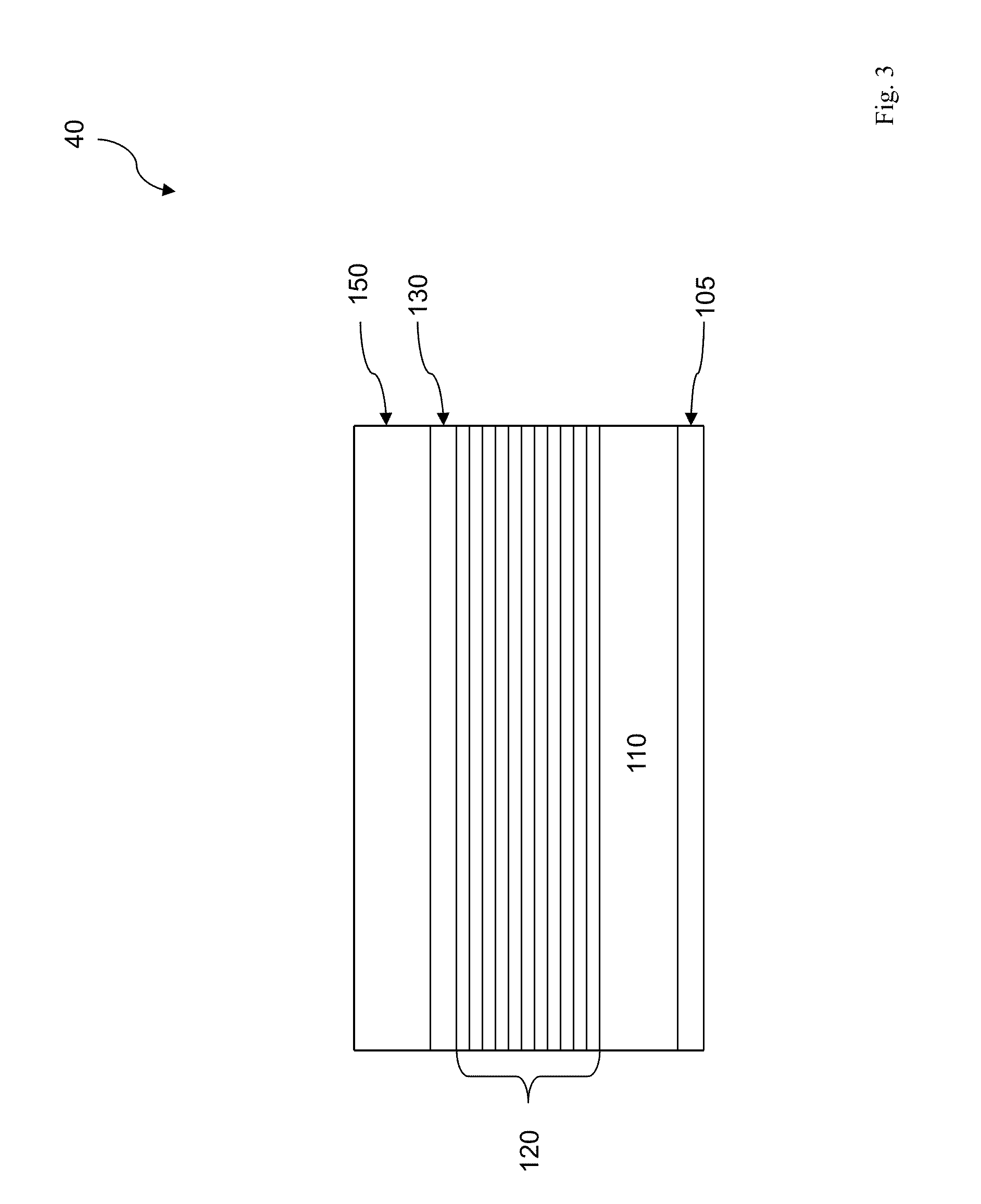
[0034]Referring back to FIG. 3, one or more of the layers 105, 120, 130, and 150 (such as 151 in FIG. 1 or 152-170 in FIG. 5) may be formed by various methods, including physical vapor deposition (PVD) process such as evaporation and DC magnetron sputtering, a plating process such as electrode-less plating or electroplating, a chemical vapor deposition (CVD) process such as a...


PUM

PropertyMeasurementUnit
thicknessaaaaaaaaaa
thicknessaaaaaaaaaa
thicknessaaaaaaaaaa

Abstract

A method of forming a mask for semiconductor fabrication is disclosed. The method includes providing a substrate and forming a first reflective layer over the substrate, wherein the first reflective layer comprises pairs of alternating materials. The method further includes forming a buffer layer over the first reflective layer and forming a second reflective layer over the buffer layer. The second reflective layer has a total thickness less than 90 nanometer (nm). The method further includes patterning the second reflective layer to form a first state and a second state of the mask. A first reflection coefficient of the first state and a second reflection coefficient of the second state have a phase difference of about 180 degrees.

Description

PRIORITY DATA[0001]This is a divisional of U.S. application Ser. No. 14 / 221,555, filed Mar. 21, 2014, entitled “An Extreme Ultraviolet Lithography Process and Mask with Reduced Shadow Effect and Enhanced Intensity,” which claims the benefit of U.S. Ser. No. 61 / 907,882 filed Nov. 22, 2013. The entire disclosure of both applications is hereby incorporated by reference.BACKGROUND[0002]The semiconductor integrated circuit (IC) industry has experienced exponential growth. Technological advances in IC materials and design have produced generations of ICs where each generation has smaller and more complex circuits than the previous generation. In the course of IC evolution, functional density (i.e., the number of interconnected devices per chip area) has generally increased while geometry size (i.e., the smallest component (or line) that can be created using a fabrication process) has decreased. This scaling down process generally provides benefits by increasing production efficiency and l...

Claims


Application Information

Patent Timeline
Patent Type & Authority Applications(United States)
IPC IPC(8): G03F1/24G03F1/76G03F7/20
CPCG03F1/24G03F1/76G03F7/2004G03F1/22G03F1/26G03F1/36H01L21/0275G03F7/2002
Inventor LU, YEN-CHENGYU, SHINN-SHENGCHEN, JENG-HORNGYEN, ANTHONY
Owner TAIWAN SEMICON MFG CO LTD
Why Eureka
Try Eureka