A method for microvia filling by copper electroplating with TSV technology for 3D copper interconnection at high aspect ratio

a technology of copper electroplating and microvia, applied in the direction of basic electric elements, electrical equipment, semiconductor devices, etc., can solve the problems of affecting the reliability of interconnection, holes in the channel, and unsatisfactory effects, and achieve the effect of high-precision dc electroplating

Inactive Publication Date: 2016-06-30
SHANGHAI SINYANG SEMICON MATERIALS
View PDF3 Cites 17 Cited by
  • Summary
  • Abstract
  • Description
  • Claims
  • Application Information

AI Technical Summary

Benefits of technology

[0031]FIG. 4 is the X-ray detection effect a schematic diagram of the invention.
[0032]The following illustration with figures will make a further description to the embodiments of this present invention.
[0033]As shown in FIG. 1 and FIG. 2, the present invention provides the method for TSV microvia filling by copper electroplating for a 3D copper interconnection at a high aspect ratio, it need to electroplate copper filling in the TSV holes shown in the figures. The used power supply is the high precision DC electroplating power.
[0034]The method provided in the present invention for microvia filling by copper electroplating with a TSV technology for a 3D copper interconnection at a high aspect ratio, comprises:
[0035]Step 1: formulating an electroplating solution of a copper methyl sulfonate system, which contains by quality volume ratio: 30-130 g / L of copper ions and 5-50 g / L of methanesulfonic acid as well as 20-150 mg / L of chlorine ions.
[0036]The electroplating solution also contains by volume ratio: 1-30 mg / L of accelerator, 5-50 mg / L of inhibitor and 1-30 mg / L of leveling agent.

Problems solved by technology

However, after testing many traditional copper plating systems, the effect has not been satisfactory.
Seams, voids, electrolyte impurities and other defects may affect the reliability of interconnection.
If the deposition rate of the upper part of the channel is higher than the lower part, there will be holes in the channel.

Method used


Image

  • A method for microvia filling by copper electroplating with TSV technology for 3D copper interconnection at high aspect ratio
  • A method for microvia filling by copper electroplating with TSV technology for 3D copper interconnection at high aspect ratio
  • A method for microvia filling by copper electroplating with TSV technology for 3D copper interconnection at high aspect ratio

Examples


example 1

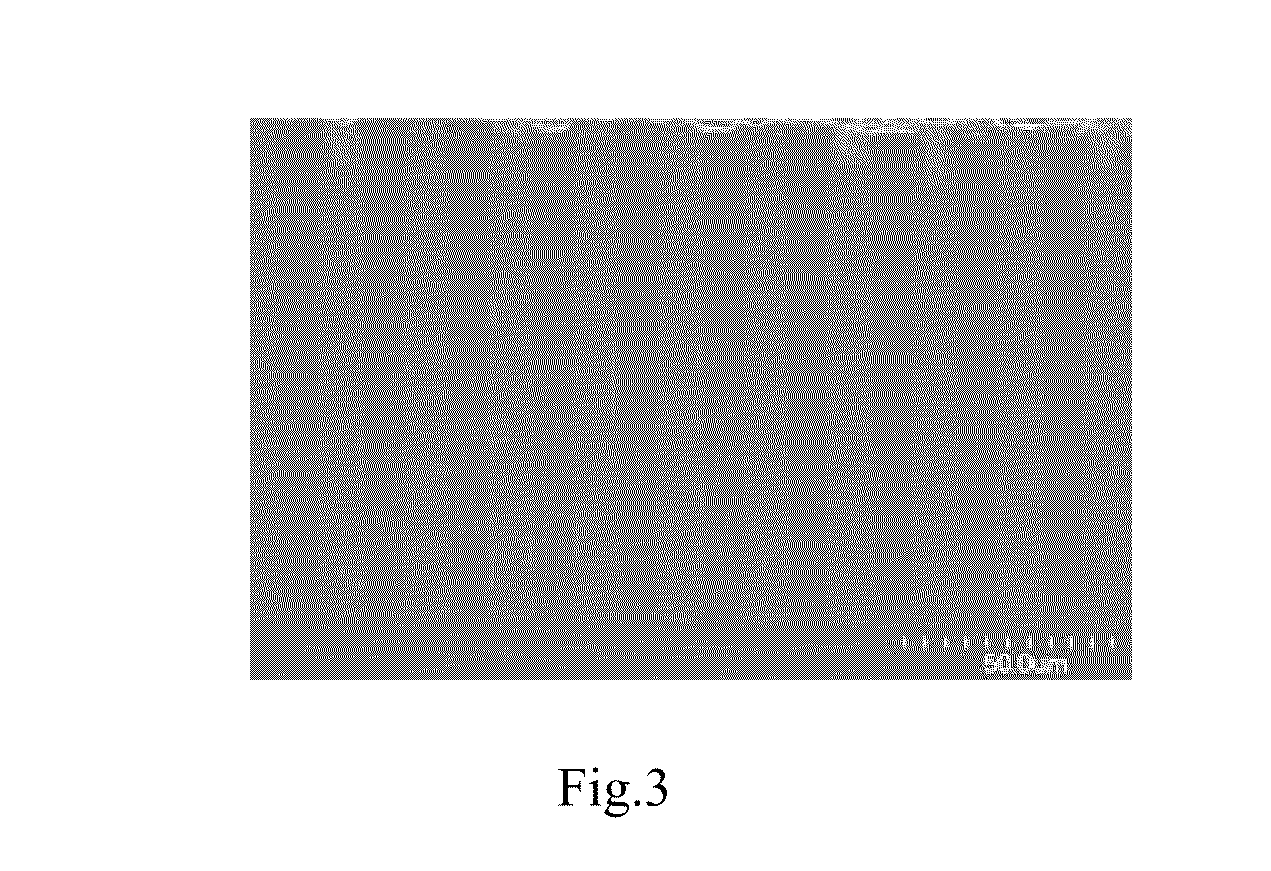
[0051]Take 10×100 μm holes for example.

[0052]Pre-treatment: vacuumize for 5 minutes at the vacuum degree of 0-0.2 torr, and immerse with pure water for 1-10 minutes.

[0053]Based methanesulfonic acid plating solution preparation: 100 g / L Cu2+, 30 g / L ultra-pure methanesulfonic acid and 30 mg / L Cl-.

[0054]Additive preparation: Accelerator: inhibitor: leveling agent =5:10:5

[0055]Experiment conditions: temperature =25° C.; Flow =15 L / min; cathode rotation =50 RPM.

[0056]Electroplating parameters: 0.01ASD 120s; 0.1ASD 600s; 0.4ASD 3000s

[0057]Results: see FIG. 3, Fully filling, no default, copper layer thickness <3 μm.

example 2

[0058]Take 15×150 μm holes for example.

[0059]Pre-treatment: vacuumize for 5 minutes at the vacuum degree of 0-0.2 torr, and immerse with pure water for 1-10 minutes.

[0060]Based methanesulfonic acid plating solution preparation: 90 g / L Cu2+, 20 g / L ultra-pure methanesulfonic acid and 20 mg / L Cl-.

[0061]Additive preparation: Accelerator: inhibitor: leveling agent =3:10:7

[0062]Experiment conditions: temperature =22-25° C.; Flow =15 L / min; cathode rotation =50 RPM.

[0063]Electroplating parameters: 0.01ASD 120s; 1.0 ASD 300s; 0.7ASD 600s; 0.5ASD 2400s; 0.7ASD 300s; 0.3ASD 1200s

[0064]Results: see FIG. 4, full filling without default

[0065]Treatment after electroplating: Wash the wafer with deionized water for 2 minutes and dry it.

[0066]Analysis, test and evaluation of the plating samples obtained from the example 1 and example 2:

[0067]1. Section analysis: make sections from the samples according to the hole patterns, seal the samples with specific epoxy curing material for polishing and chec...


PUM

PropertyMeasurementUnit
temperatureaaaaaaaaaa
current densityaaaaaaaaaa
depthaaaaaaaaaa

Abstract

A method for microvia filling by copper electroplating with a TSV technology for a 3D copper interconnection at a high aspect ratio, which includes: Step 1: formulating an electroplating solution of a copper methyl sulfonate system, Step 2: wetting the microvias of the TSV technology by means of an electroplating pre-treatment, Step 3: charging into the grooves, completing the ultra-low current diffusion, so that the copper ions and the additives are rationally distributed at the surface and the interior of the microvias of the TSV technology, Step 4: connecting the wafer for the TSV technology to the cathode of a power source, fully immersing the electroplating surface of the wafer in the electroplating solution, and electroplating with a step-by-step current method of rotating or stirring the cathode, the current density of the plating conditions is 0.01-10A/dm2 and the temperature is 15-30° C., Step 5: after the electroplating, washing the wafer completely clean with deionized water, and drying it by spinning or blowing. The method for microvia filling by copper electroplating with a TSV technology for a 3D copper interconnection at a high aspect ratio has a high via-filling speed, a thin copper layer on the surface, no risk of creating voids and cracks, and can achieve the complete filling of microvias having an aspect ratio of more than 10:1 which are extremely difficult to fill.

Description

TECHNICAL FIELD[0001]This invention involves a method micro-electroplating method of copper plating step by step for 3D TSV technology, in particular, relates to a method for microvia filling by copper electroplating with TSV technology for 3D copper interconnection at high aspect ratio.BACKGROUND ART[0002]TSV (Through-Silicon-Via) technology is the latest technology of making vertical breakover between chips, and wafers to realize the interconnection between chips. Different from the IC packaging bonding and the superposition technique using convex points, TSV can make the chips stacked in the three-dimensional directions of the maximum density, the minimum size, and significantly improve the operation speed of the chips and reduce power consumption.[0003]Since the copper electroplating deposition process has been widely used in the semiconductor technology, it is believed that the technique could be transformed from copper damascene to through-hole filling TSV. However, after test...

Claims


Application Information

Patent Timeline
Patent Type & Authority Applications(United States)
IPC IPC(8): H01L21/768C25D5/48C25D5/34C25D7/12C25D3/38
CPCH01L21/76879C25D7/12C25D3/38H01L21/76898C25D5/48H01L21/76883C25D5/34H01L21/2885
Inventor WANG, SUYU, XIANXIANMA, LILI, YANYAN
Owner SHANGHAI SINYANG SEMICON MATERIALS
Why Eureka
Try Eureka