Oxide semiconductor substrate and schottky barrier diode

a technology of schottky barrier and semiconductor substrate, which is applied in the direction of basic electric elements, electrical equipment, semiconductor devices, etc., can solve the problems of sic from the viewpoint of mass productivity and cost, mass productivity, and difficult to obtain a crystal with a small number of dislocations, and achieve high mass productivity, excellent current-voltage characteristics, and low cost

Active Publication Date: 2016-07-21
IDEMITSU KOSAN CO LTD
View PDF2 Cites 31 Cited by
  • Summary
  • Abstract
  • Description
  • Claims
  • Application Information

AI Technical Summary

Benefits of technology

[0013]The invention was conceived in view of the above problems. An object of the invention is to provide a Schottky barrier diode element that is obtained by forming a compound semiconductor having a wide band gap on an inexpensive substrate (e.g., Si wafer) at low cost with high mass productivity, and that exhibits excellent current-voltage characteristics.
[0046]The invention thus provides a Schottky barrier diode element that is obtained by forming a compound semiconductor having a wide band gap on an Si substrate at low cost with high mass productivity, and that exhibits excellent current-voltage characteristics.

Problems solved by technology

However, since it is difficult to implement the epitaxial growth of GaAs on an Si substrate, it is difficult to obtain a crystal with a small number of dislocations.
However, since the substrate production process and the epitaxial growth process require a high-temperature process, SiC has a problem from the viewpoint of mass productivity and cost.
However, since it is necessary to use a molecular beam epitaxy method at present in order to implement homoepitaxial growth, there is a problem from the viewpoint of mass productivity.

Method used


Image

  • Oxide semiconductor substrate and schottky barrier diode
  • Oxide semiconductor substrate and schottky barrier diode
  • Oxide semiconductor substrate and schottky barrier diode

Examples


example 1

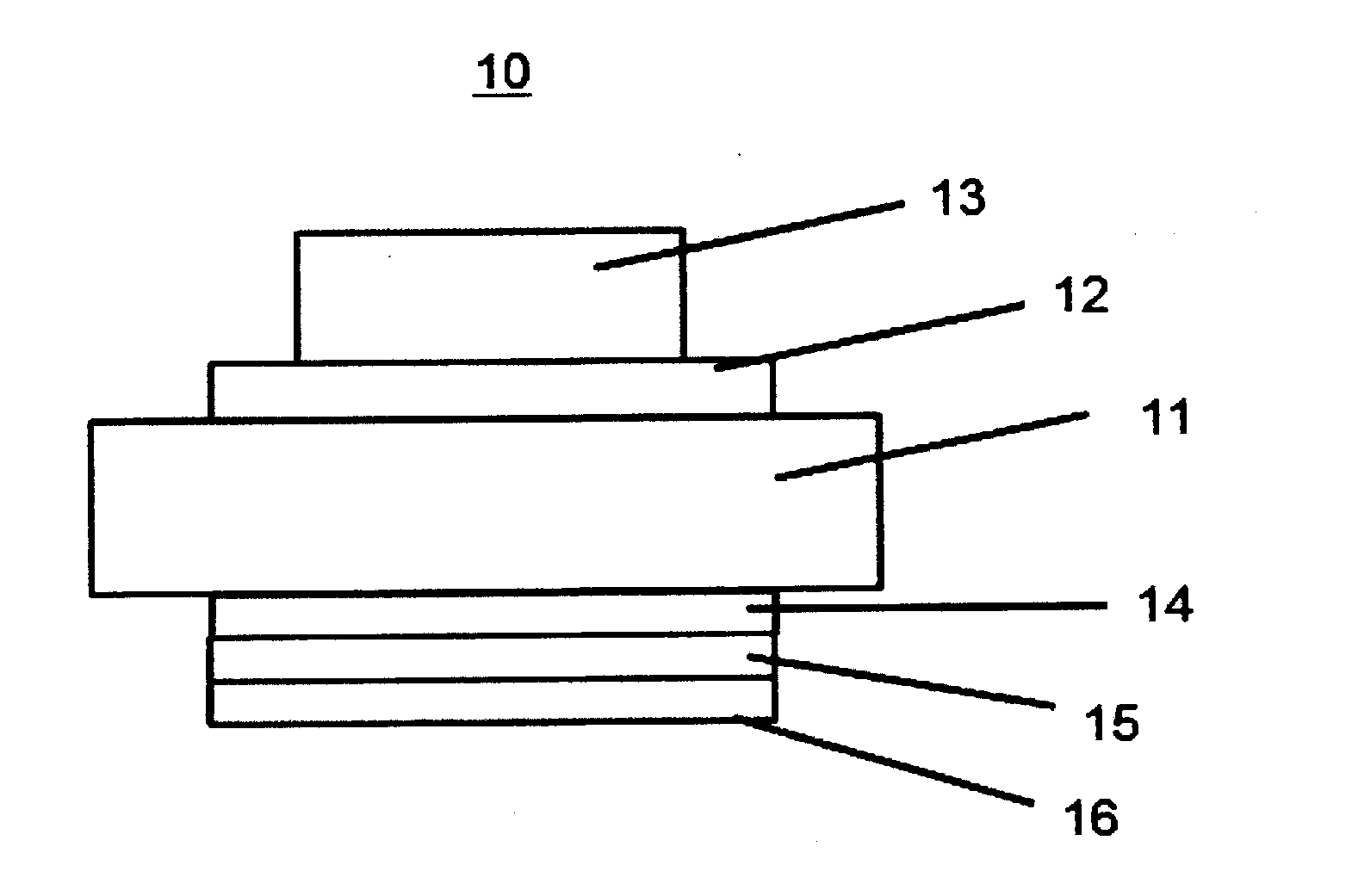
[0129]FIG. 1 is a cross-sectional view schematically illustrating a Schottky barrier diode element obtained in Example 1.

[0130]An n-type silicon (Si) substrate 11 having a resistivity of 0.02 Ω·cm was provided, and treated with diluted hydrofluoric acid to remove a natural oxide film from the surface of the substrate. The Si substrate (wafer) was placed in a sputtering device (“HSM552” manufactured by Shimadzu Corporation). A sputtering discharge was effected at an RF power of 100 W using a Ga2O3 sintered body including 500 ppm of Si (this composition is hereinafter referred to as “Si—Ga2O3”) as the sputtering target to form an Si—Ga2O3 film (gallium oxide film) 12 having a thickness of 300 nm on the surface of the Si substrate from which an oxide film was removed.

[0131]The Si—Ga2O3 film was patterned by photolithography to form the desired pattern, and annealed at 500° C. for 0.5 hours in nitrogen to effect crystallization. The crystal state of the Si—Ga2O3 film was determined by X...

examples 2 and 3

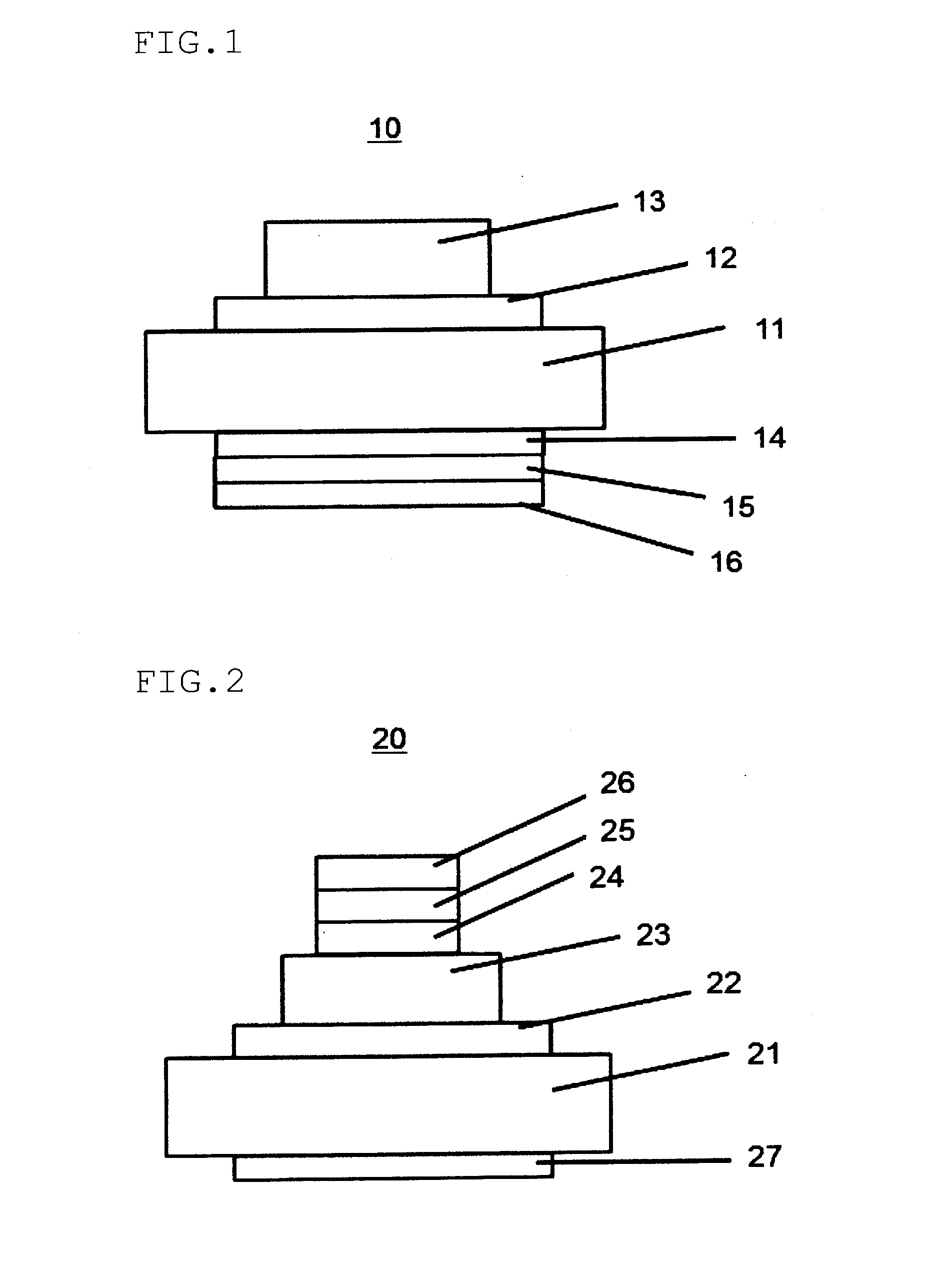
[0145]A Schottky barrier diode element was produced using a sputtering method in the same manner as in Example 1, except that the Schottky electrode and the semiconductor composition were appropriately changed as shown in Table 1. The measurement results for the current-voltage characteristics are shown in Table 1.

example 4

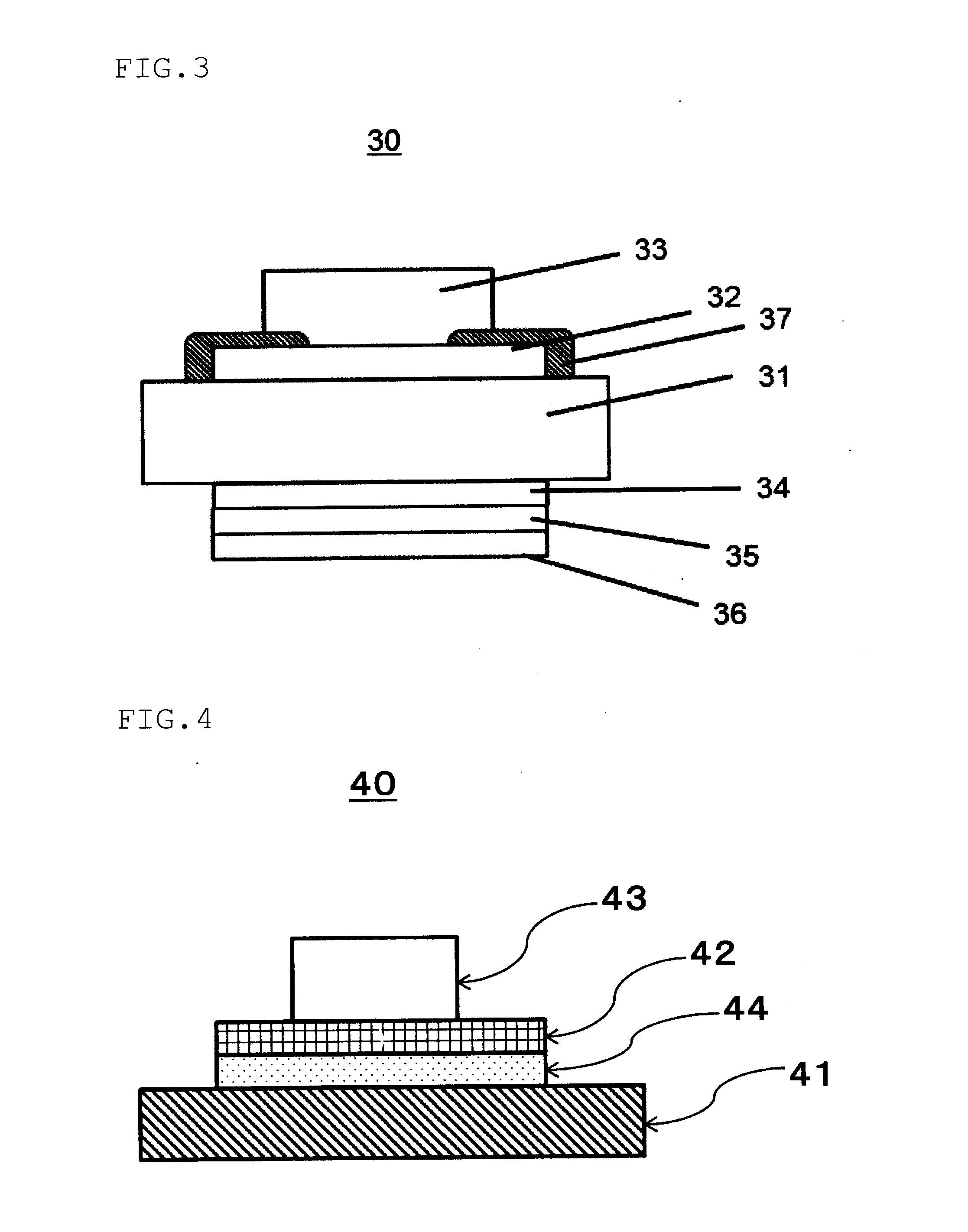
[0146]An n-type Si substrate having a resistivity of 0.02 Ω·cm was provided, and treated with diluted hydrofluoric acid to remove a natural oxide film from the surface of the substrate. The Si substrate (wafer) was placed in a sputtering device (“HSM552” manufactured by Shimadzu Corporation). Ga2O3 was used as the sputtering target. A sputtering discharge was effected at an RF power of 100 W to form a gallium oxide film having a thickness of 300 nm on the surface of the Si substrate from which an oxide film was removed.

[0147]The Si substrate (wafer) on which the gallium oxide film was formed was placed in an ion doping implantation device, and doped with Si at a concentration of 0.5 at %. The Si substrate was then annealed at 500° C. for 1 hour in air to activate Si and form a polycrystalline Ga2O3 film. The polycrystalline Ga2O3 film was patterned by photolithography to form the desired pattern. The substrate was placed in the sputtering device, and sputtering was performed using a...


PUM


Abstract

A Schottky barrier diode element includes an n-type or p-type silicon (Si) substrate, an oxide semiconductor layer, and a Schottky electrode layer, the oxide semiconductor layer including either or both of a polycrystalline oxide that includes gallium (Ga) as the main component and an amorphous oxide that includes gallium (Ga) as the main component.

Description

TECHNICAL FIELD[0001]The invention relates to an oxide semiconductor substrate and a Schottky barrier diode element that have rectifying characteristics.BACKGROUND ART[0002]A Schottky barrier diode is a diode that produces a rectifying action utilizing a potential barrier formed at the junction between a metal and a semiconductor. Si is most widely used as the semiconductor (see Patent Literature 1, for example). As a compound semiconductor having a band gap wider than that of Si, GaAs and, recently, SiC may be used instead of Si (see Patent Literatures 2 and 3, for example).[0003]An Si-based Schottky diode is used for a high-speed switching element, a GHz-band transmission / reception mixer, a frequency conversion element, and the like. A GaAs-based Schottky diode can implement a higher-speed switching element, and is used for a microwave converter, a microwave mixer, and the like. It is considered that SiC can be applied to the electric vehicle field, the railroad field, the power t...

Claims


Application Information

Patent Timeline
Patent Type & Authority Applications(United States)
IPC IPC(8): H01L29/872H01L29/47H01L29/24
CPCH01L29/872H01L29/47H01L29/24H01L29/247H01L29/26H01L29/04H01L29/16H01L29/267
Inventor TOMAI, SHIGEKAZUSHIBATA, MASATOSHIKAWASHIMA, EMIYANO, KOKIHAYASAKA, HIROMI
Owner IDEMITSU KOSAN CO LTD
Why Eureka
Try Eureka