Diamond substrate and diamond substrate manufacturing method

a diamond substrate and manufacturing method technology, applied in the direction of crystal growth process, polycrystalline material growth, after-treatment details, etc., can solve the problems of difficult to apply the processing device to a small substrate less than several inches, complicated process of manufacturing a semiconductor device, limited practical area, etc., to prevent the formation of cracks in the diamond substrate layer, the effect of easy manufacturing

Active Publication Date: 2016-08-18
NAMIKI PRECISION JEWEL CO LTD
View PDF1 Cites 1 Cited by
  • Summary
  • Abstract
  • Description
  • Claims
  • Application Information

AI Technical Summary

Benefits of technology

[0022]According to the diamond substrate of the present invention, it is possible to realize a large diamond substrate with a diameter of two inches or more which is formed of diamond single crystals.
[0023]According to the diamond substrate manufacturing method of the present invention, the diamond single crystals growing from the pillar-shaped diamonds are coalesced to manufacture a diamond substrate layer. Accordingly, by increasing the number of pillar-shaped diamonds, it is possible to easily manufacturing a large-diameter diamond substrate layer with a diameter of two inches or more.
[0024]According to the diamond substrate manufacturing method of the present invention, a stress is generated in each pillar-shaped diamond due to a difference in lattice constant and / or a difference in thermal expansion coefficient between the base substrate and the diamond substrate layer when the diamond substrate layer is grown, and the pillar-shaped diamonds are destroyed by the stress to separate the diamond substrate layer from the base substrate.
[0025]Accordingly, even when a stress generated in the diamond substrate layer increases with an increase in size, the stress of the diamond substrate layer is released toward the outside by destruction of the pillar-shaped diamonds and thus formation of a crack in the diamond substrate layer is prevented. In this respect, it is also possible to manufacture a large diamond substrate.
[0026]By manufacturing the diamond substrate from the diamond substrate layer, it is possible to manufacture a large-diameter diamond substrate with a diameter of two inches or more.

Problems solved by technology

This is because when a processing device which is used for micro-machining of a general semiconductor such as Si is applied to a diamond, it is difficult to apply the processing device to a small substrate less than several inches.
However, coupling boundaries are formed as areas in which crystal quality deteriorates on the boundaries between the diamond single crystal substrates arranged in the shape of tiles.
Since the part of the coupling boundary cannot be used for growth of a semiconductor device, an area which can be used in practice is limited with respect to the area of the diamond single crystal substrate which is obtained by the mosaic growth method.
To make matters worse, the area of the diamond single crystal substrate which can be used to manufacture a semiconductor device does not match the size of a semiconductor device chip necessarily.
As a result, the process of manufacturing a semiconductor device is complicated.
However, a stress is generated in crystals of a diamond substrate formed by growth due to a difference in lattice constant and thermal expansion coefficient between the base substrate and the diamond and thus a warp or a crack is generated in the diamond substrate.
Accordingly, it is not easy to obtain a large substrate using the heteroepitaxial growth method.

Method used


Image

  • Diamond substrate and diamond substrate manufacturing method
  • Diamond substrate and diamond substrate manufacturing method
  • Diamond substrate and diamond substrate manufacturing method

Examples


Embodiment Construction

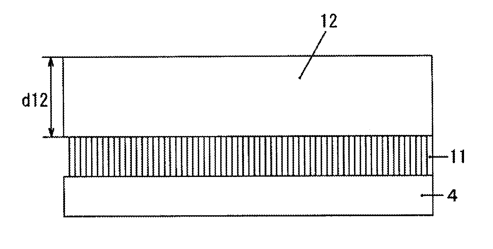
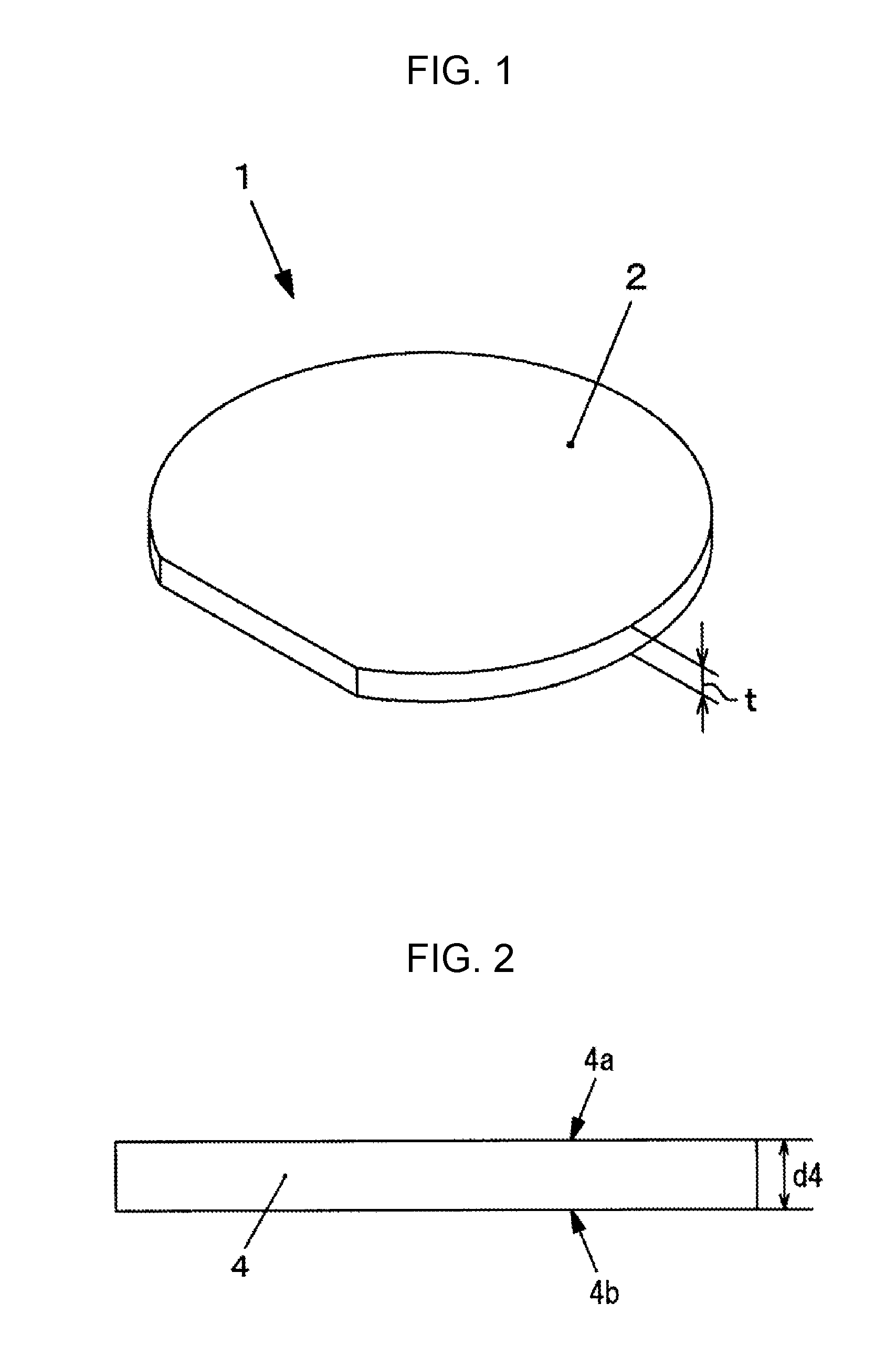
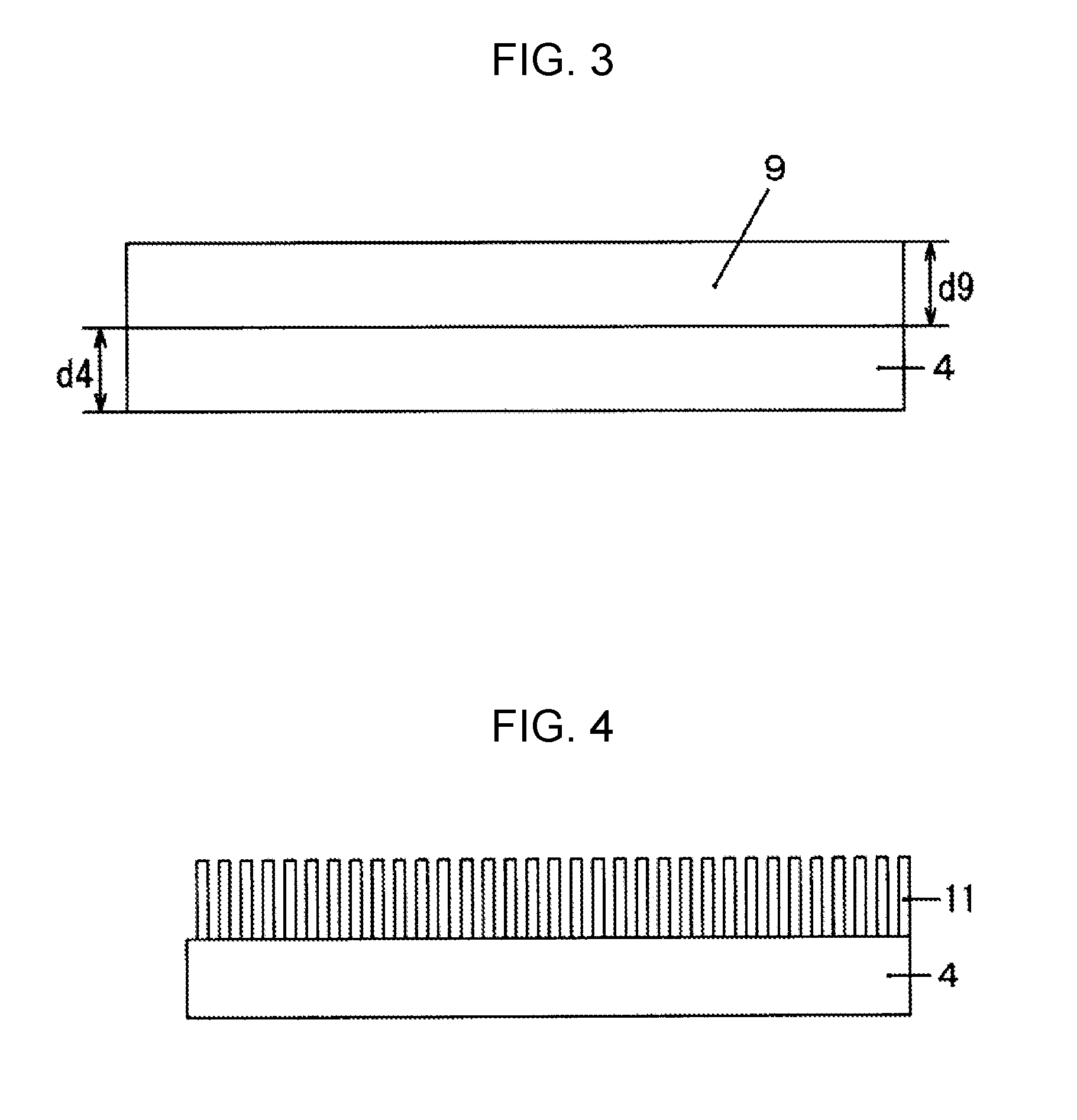
[0037]Hereinafter, a diamond substrate according to the present invention will be described in detail with reference to FIG. 1. The shape in an in-plane direction of the diamond substrate according to the present invention is not particularly limited and may be, for example, a rectangular shape. However, a circular shape can be preferably used from the viewpoint of easy use in manufacturing processes for a surface acoustic wave element, a thermistor, a semiconductor device, and the like. Particularly, as illustrated in FIG. 1, a circular shape having an orientation flat plane formed therein can be preferably used.

[0038]When the shape of the diamond substrate 1 is a circular shape or a circular shape having an orientation flat plane formed therein as illustrated in FIG. 1, the diameter is preferably equal to or greater than two inches (about 50.8 mm) from the viewpoint of an increase in size of a practical substrate, more preferably equal to or greater than three inches (about 76.2 m...


PUM

PropertyMeasurementUnit
diameteraaaaaaaaaa
diameteraaaaaaaaaa
surface roughnessaaaaaaaaaa

Abstract

A diamond substrate is formed of diamond single crystals by preparing a base substrate; forming plural pillar-shaped diamonds formed of diamond single crystals on one side of the base substrate; causing a diamond single crystal to grow from a tip of each pillar-shaped diamond and coalescing the diamond single crystals growing from the tips of the pillar-shaped diamonds to form a diamond substrate layer; separating the diamond substrate layer from the base substrate; and manufacturing a diamond substrate from the diamond substrate layer, a shape in an in-plane direction of the diamond substrate is a circular shape or a circular shape having an orientation flat plane formed therein and has a diameter of two inches or more.

Description

TECHINICAL FIELD[0001]The present invention relates to a diamond substrate and a diamond substrate manufacturing method.BACKGROUND ART[0002]A diamond is expected to be an ultimate semiconductor substrate. This is because a diamond has a lot of excellent characteristics, which are unparalleled in anywhere as a semiconductor material, such as high thermal conductivity, high electron / hole mobility, high dielectric breakdown field strength, low dielectric loss, and a wide bandgap. The bandgap thereof is about 5.5 eV which is a very high value in existing semiconductor materials. Particularly, in recent years, UV light emitting elements using a wide bandgap, field effect transistors having excellent high-frequency characteristics, and the like have been developed.[0003]When it is considered that a diamond is used as a semiconductor, a certain size such as a diameter of several inches is required. This is because when a processing device which is used for micro-machining of a general semi...

Claims


Application Information

Patent Timeline
Patent Type & Authority Applications(United States)
IPC IPC(8): C30B25/18C30B33/02C30B29/04C30B25/10
CPCC30B29/04C30B25/105C30B33/02C23C16/01C23C16/274C30B25/18H01L21/02376H01L21/8206
Inventor AIDA, HIDEOKOYAMA, KOJIIKEJIRI, KENJIROKIM, SEONGWOO
Owner NAMIKI PRECISION JEWEL CO LTD
Why Eureka
Try Eureka