GE Energy Power Conversion Technology Ltd

a technology of power conversion and energy, applied in the field of power electronic modules, can solve the problems of short circuit between, damage to drive units and other system components, and inability to control functionally capable switching elements through gate electrodes, etc., and achieve the effects of avoiding or at least reducing damage, low control power, and high blocking voltag

Active Publication Date: 2016-09-08
GE ENERGY POWER CONVERSION TECH
View PDF2 Cites 18 Cited by
  • Summary
  • Abstract
  • Description
  • Claims
  • Application Information

AI Technical Summary

Benefits of technology

[0015]Embodiments of the present invention are based on the idea that, in case of a fault in one or more of the switching elements in the switch module, the fault protection device automatically controls at least some of the non-faulty or functionally capable switching elements to switch to a conducting state or maintains them in a conducting state before they are damaged or destroyed as a result of the short circuit fault, e.g., as a result of overcurrent, heat build-up, electric arc etc. This protection is provided in purely passive manner, and in particular without any additional active logic, active control or active switching, and without additional active connections or changeover of current paths or other additional measures. The functionally capable switching elements remain controllable and in a conducting state so that a stable low Ohm (low impedance) current path is created through the switch module and the danger of an explosion and damage being caused is avoided or at least reduced.
[0016]In an embodiment, the switching elements are power semiconductor devices, e.g., voltage-controlled power semiconductor devices such as IGBTs, MOSFETS and junction field effect transistors (JFETs). IGBTs can be implemented due to their low control power, high blocking voltage, robustness against short circuits and their suitability to be connected in series and / or in parallel.
[0017]The switch module can further comprise a housing accommodating all of the switching elements. The first and the second connections and the at least one control connection extend outside the housing. The housing can be a pressure contact housing (e.g., a so-called “press-pack” housing) in which the semiconductor chips are pressed between pressure contact plates. In the case of a gate-emitter short circuit fault in an IGBT, the collector-emitter-short circuit is secured through pressure contact of the semiconductor chip for an intermediate period, i.e., at least in the range of hours or days. The fault protection device is able to secure the short circuit for a longer period, i.e., several months or years. The housing can also be a module-type housing in which the semiconductor chips are bonded. In a fault situation the bond wires of the faulty semiconductor chips can lift off the chip, which can lead to explosion. This process can happen within fractions of a second after chip failure. The fault protection device with its passive protection network is able to act essentially without delay in order to switch non-faulty switching elements to a conducting state or to maintain them in a conducting state.

Problems solved by technology

If one of the parallel connected switching elements, for example, an IGBT, suffers a short circuit between its collector electrode and its emitter electrode, and as a result becomes faulty and is destroyed, this generally leads to a short circuit between the gate electrode of the switching element and its emitter electrode.
The gate-emitter short circuit of the faulty switching element, due to parallel switching, also shorts the gate electrodes of other, functionally capable switching elements to the emitter electrode and prevents the gate electrodes from maintaining a sufficient voltage so as to remain in a conducting state or to move to a conducting state.
Consequently, a control of the functionally capable switching elements is impossible through the gate electrodes.
The current load of the faulty switching element with nominal current of the switch module or possible overcurrent, and the associated excessive heating, can lead to destruction of the switch module and also damage the drive unit and other system components.
Especially, electric arcs can emerge, which can lead to outage of other components, an explosion of components or fire.
In order to avoid a mechanical destruction of the switch module through explosion, the switching elements so far have been protected against explosion by explosion-proof metal housings, which is difficult and expensive.
Due to material oxidation, if the electrical resistance of the damaged switching element increases, another electrically parallel connected switching element will be damaged and it melts and forms the next low Ohm (or low impedance) current path.
In spite of the high complexity, a continuous and stable short circuit failure mode cannot be ensured.
However, this solution requires an additional active switch within the switch module and an active logic for controlling this additional active switch in case of fault.

Method used


Image

  • GE Energy Power Conversion Technology Ltd
  • GE Energy Power Conversion Technology Ltd
  • GE Energy Power Conversion Technology Ltd

Examples


first embodiment

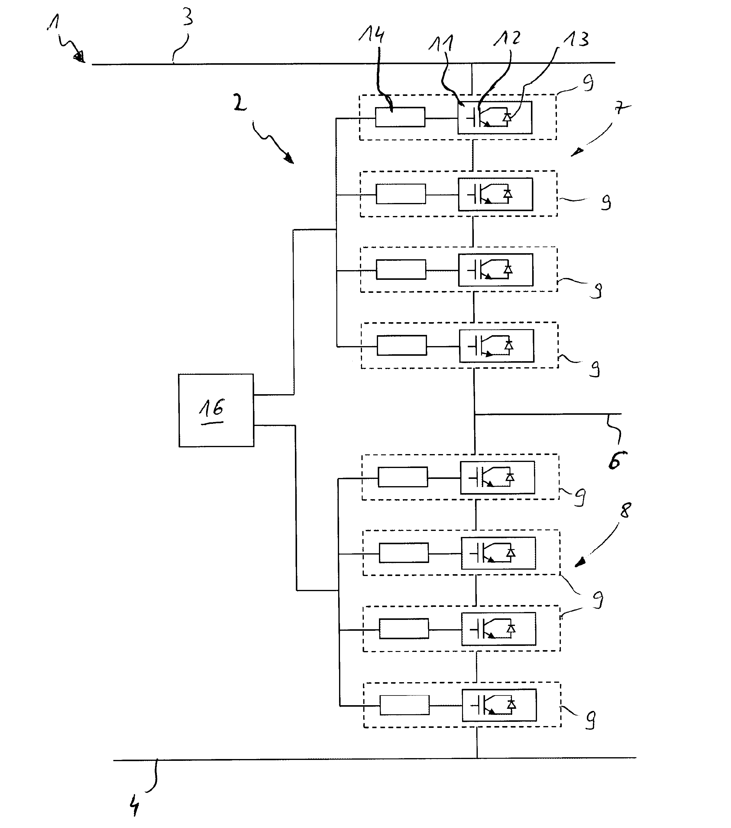
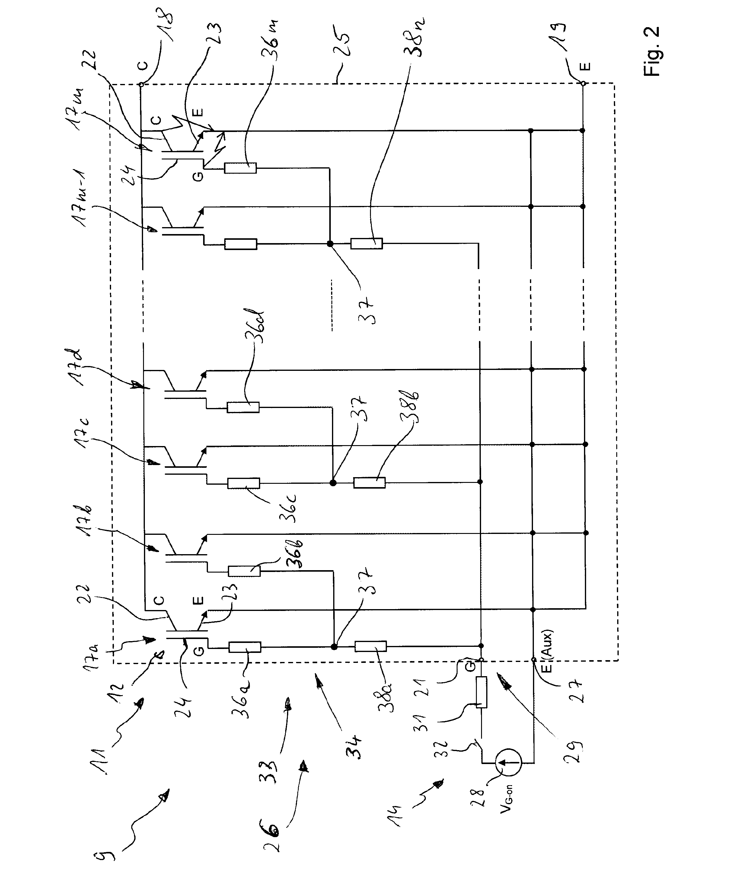
[0052]FIG. 2 shows a block image of a power electronic module 9, which includes a switch module 11 and a drive unit 14. As illustrated, the switch module 11 includes a plurality of switching elements 17a, 17b, 17c, 17d 17m−1, 17m, which are connected in parallel between a first connection 18, a second connection 19, and a control connection 21. The switch module 11 can include any suitable number of switching elements, but typically a minimum of two switching elements are arranged in parallel with each other.

[0053]In an embodiment, the switching element 17 may be a power semiconductor device, e.g., an IGBT, MOSFET, JFET or similar controllable power semiconductor switch, which can be switched between a conducting state and a non-conducting (or blocking) state through suitable control. In the Figs., for simplification of the following description, IGBTs are illustrated as the switching elements 17 and the associated free-wheeling diodes are omitted. In the following description the ...

second embodiment

[0074]FIG. 3 shows a power electronic module 9, which includes a switch module 11 according to a The switch module 11 is similar to the switch module shown in FIG. 2 but the second resistances 38 have been omitted so that the first resistances 36 are connected through the connection points 37 directly to the gate connection 21.

[0075]Through suitable design of the resistance matrix 34 it can be ensured that, for a given drive voltage VG-on, which is applied by the drive unit 14 through a drive resistance 31 to the connections 19, 21 of the switch module 11, the gate-emitter voltage at the gate electrodes 24 of functionally capable, non-faulty switching elements 17 is greater than the threshold voltage VGE-th.

[0076]As an example, for the switch module 11 shown in FIG. 3, under the assumption that the electrical resistances of the first resistances 36 between the gate connection 21 and the gate electrodes 24 are substantially equal, i.e., so Rint=R11=R12= . . . =R1m, the following con...

third embodiment

[0080]FIG. 4 shows a switch module 11 according to a The switch module 11 is similar to the switch module shown in FIG. 2 but a fuse 39a, 39b, . . . , 39n is provided in each gate current path between the gate electrode 24 of each switching element 17 and the respective connecting point 37 for the group of switching elements. As shown in FIG. 4, each fuse 39 is connected between a first resistance 36 and the connecting point 17 for the group of switching elements. The fuses 39 can be safety fuses or resettable fuses, and depending on the resistance matrix 34, are designed or selected in such a way that they trigger in the event of a fault in order to separate the short-circuited gate electrode 24 of a faulty switching element 17 from the gate connection 21, whereas the other fuses associated with the non-faulty switching elements 17 are not affected.

[0081]In cases of a short-circuited gate structure of a faulty switching element, the resultant gate current, which is fed with the ap...


PUM


Abstract

A switch module includes a collector connection, an emitter connection, and a gate connection. The switch module includes a plurality of parallel connected switching elements, e.g., insulated-gate bipolar transistors, each having a collector electrode electrically connected to the collector connection, an emitter electrode electrically connected to the emitter connection, and a gate electrode electrically connected to the gate connection. A fault protection device is operatively electrically connected between the gate connection and the switching elements and comprises passive electrical components which are selected such that in the event of a fault in at least one of the plurality of switching elements, a gate-emitter voltage is provided to the gate electrodes of non-faulty switching elements in a passive manner.

Description

TECHNICAL FIELD[0001]The present invention relates to a switch module with short circuit failure protection and a power electronic module incorporating such a switch module.BACKGROUND ART[0002]Switch modules with power semiconductor devices are used in converters for the conversion of direct current (DC) to alternating current (AC) and vice versa, and for many other applications. A switch module represents a controllable part, whose state can be changed by a control signal between a conducting (or on) state and a non-conducting (or off) state. For high performance applications, for example, high voltage-direct current (HVDC) applications, in many multi-level converter topologies, often several switch modules are connected to each other in series. Redundancy requirements, according to which the function of a device must be ensured in case of a failure of one or more switch modules, can require the application of two or more switch modules connected in series.[0003]It is important tha...

Claims


Application Information

Patent Timeline
Patent Type & Authority Applications(United States)
IPC IPC(8): H02M1/32H02M7/537
CPCH02M7/537H02M1/32H03K17/08H03K17/12H03K17/08104H03K17/08116H03K17/08142H03K17/08148H03K17/0822H03K17/0828H02M1/088H02M1/325
Inventor BRUECKNER, THOMASJAKOB, ROLAND
Owner GE ENERGY POWER CONVERSION TECH
Why Eureka
Try Eureka