Organic electroluminescent element, electronic device, light emitting device, and light emitting material

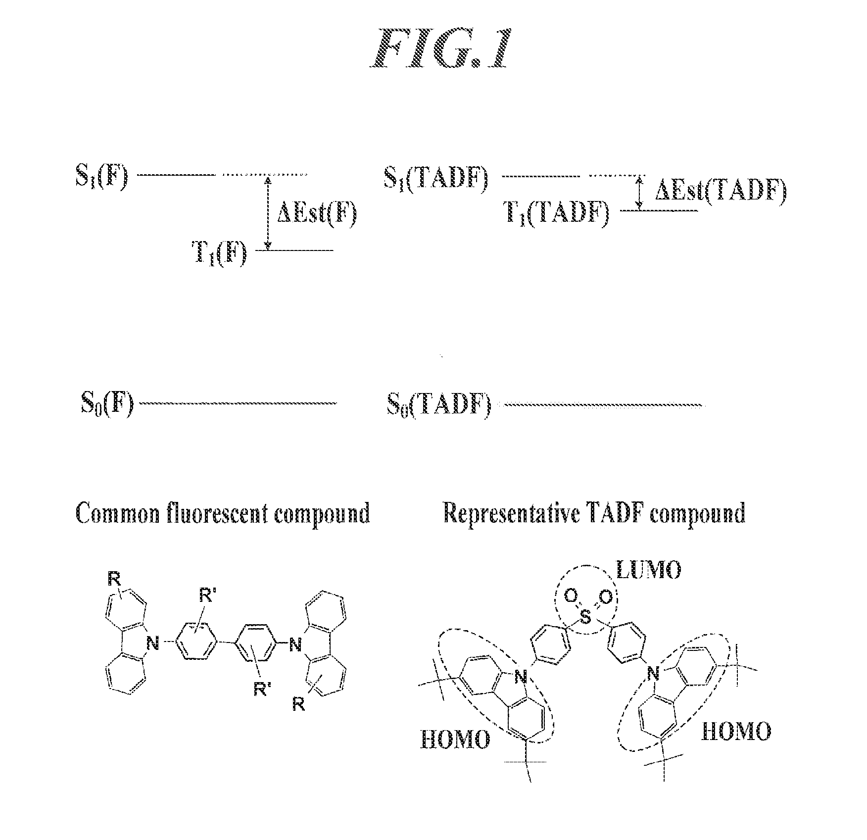
a technology of electroluminescent elements and light emitting materials, applied in the direction of luminescent compositions, organic chemistry, chemistry apparatus and processes, etc., can solve the problems of reducing the amount of rare metal deposits or the cost of rare metal deposits in the future, the emission efficiency of tta is not as high as that of the aforementioned phosphorescent materials, etc., to achieve high emission efficiency, long life, and high emission efficiency

Inactive Publication Date: 2016-09-15
KONICA MINOLTA INC
View PDF2 Cites 62 Cited by
  • Summary
  • Abstract
  • Description
  • Claims
  • Application Information

AI Technical Summary

Benefits of technology

[0046]By the above-described embodiments of the present invention, it is possible to provide an organic electroluminescent element achieving high emission efficiency with a long lifetime, and to provide an electronic device and a light emitting device provided with the organic electroluminescent element. Further, it is possible to provide a light emitting material achieving high emission efficiency with a long lifetime.
[0047]A formation mechanism or an action mechanism of the effects of the present invention is not clearly identified, but it is supposed as follows.
[0048]For the purpose of effectively driving an organic EL element, when a fluorescent compound and a host compound are used together, the used compounds are selected on the premise that energy is transferred from the host compound to the fluorescent compound.
[0049]However, when a fluorescent compound having a large emission region in the UV region is used, it may occur energy transfer from the fluorescent compound to the host compound, this energy transfer is normally not expected and it does not contribute to an emission of the element.
[0050]As a result of this unexpected energy transfer, an emission efficiency of an element will be decreased, and further, an amount of the host compound at an excited state, namely, in the high reactive state, will be increased. Further, this high reactive host compound at an excited state will modify the physical property of the organic layer composing the light emitting layer by the reaction with the same species or by the reaction with other quencher. This will lead to an unwanted effect such as the degradation of lifetime of the element at the end.
[0051]In the present invention, it was focused on the fact that a emission component in the UV region can be reduced by using a fluorescent compound having a half bandwidth in the specific range among the fluorescent compounds. As a result, the unexpected energy transfer from the fluorescent compound to the host compound can be inhibited, and it can be obtained an organic electroluminescent element of high efficiency with a long lifetime.

Problems solved by technology

This may induce an industrial problem of the amount of deposit or the cost of the rare metals in the future.
Although this technique can increase power efficiency of a fluorescence emission material (hereafter, it is called as a fluorescent emission material or fluorescent material) from two to three times larger than the power efficiency of a conventional fluorescent material, the emission efficiency in TTA is not as high as that of the aforementioned phosphorescent material due to a theoretical limitation, because the rate of conversion of the excited triplet energy level to the excited singlet energy level will remain to about 40%.
However, when a fluorescent compound which emits fluorescence by making use of the TADA mechanism has a large emission region in the UV region, it may produce energy transfer from the fluorescent compound to the host compound, and this energy transfer will not contribute to an emission of the organic EL element.
This will cause a problem of decreasing emission efficiency.

Method used


Image

  • Organic electroluminescent element, electronic device, light emitting device, and light emitting material
  • Organic electroluminescent element, electronic device, light emitting device, and light emitting material
  • Organic electroluminescent element, electronic device, light emitting device, and light emitting material

Examples


examples

[0382]Hereafter, the present invention will be described specifically by referring to Examples, however, the present invention is not limited to them. In Examples, the term “parts” or “%” is used. Unless particularly mentioned, it represents “mass parts” or “mass %”.

[0383]In addition, a volume % of a compound in each example is obtained from a specific gravity by measuring a produced layer thickness with a quartz oscillator microbalance method and by calculating a mass.

>

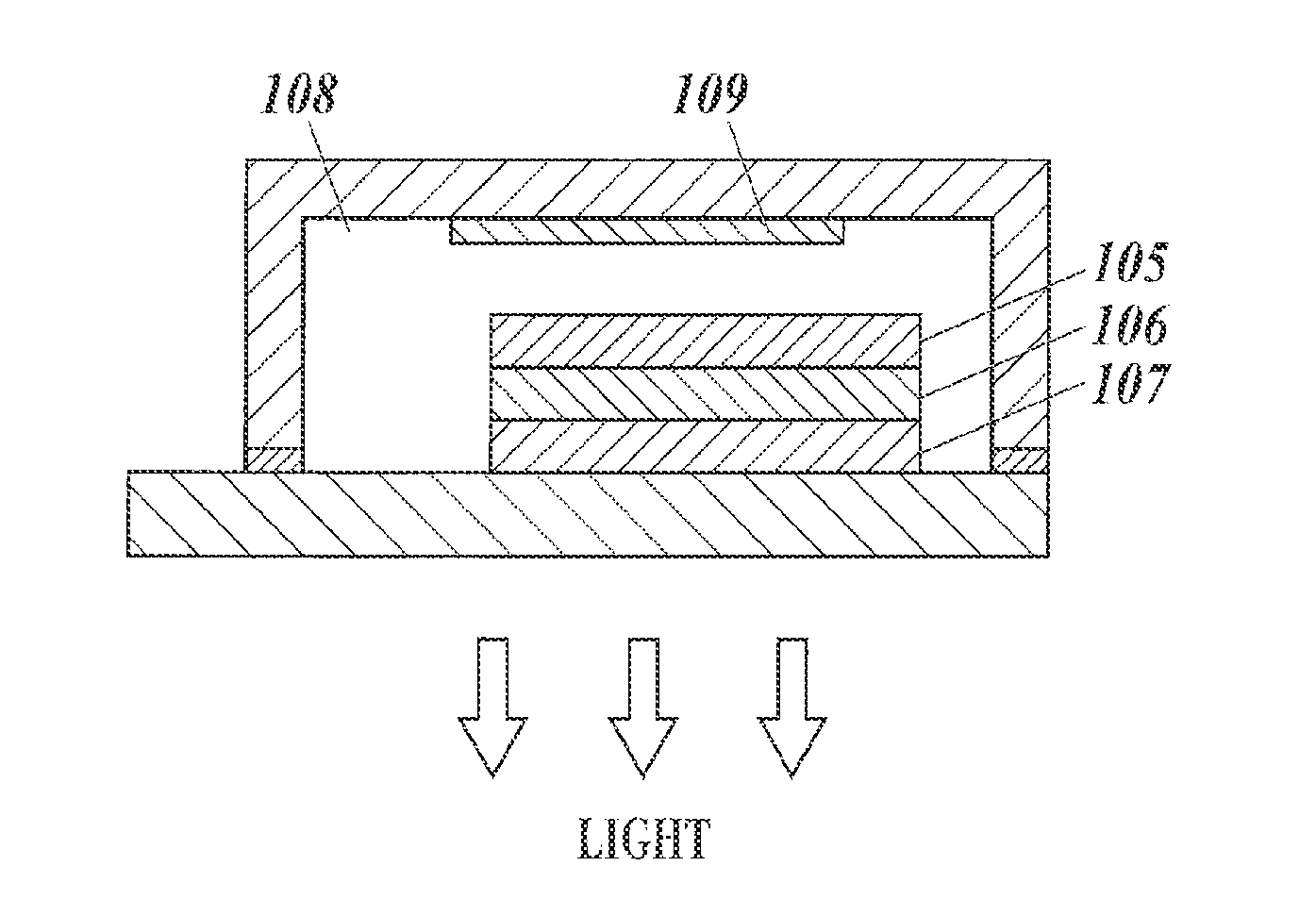
[0384]An anode was prepared by making patterning to a glass substrate of 100 mm×100 mm×1.1 mm (NA45, produced by NH Techno Glass Corp.) on which ITO (indium tin oxide) was formed with a thickness of 100 nm. Thereafter, the above transparent support substrate provided with the ITO transparent electrode was subjected to ultrasonic washing with isopropyl alcohol, followed by drying with desiccated nitrogen gas, and was subjected to UV ozone washing for 5 minutes.

[0385]On the transparent support substrate thus prepared w...


PUM

PropertyMeasurementUnit
internal quantum efficiencyaaaaaaaaaa
phosphorescence quantum efficiencyaaaaaaaaaa

Abstract

An objective of the present invention is to provide: an organic electroluminescent element which has high efficiency and a long service life; and an electronic device and a light emitting device, each of which is provided with the organic electroluminescent element. Another objective of the present invention is to provide a light emitting material which has high efficiency and a long service life. An organic electroluminescent element according to the present invention comprises at least one organic layer that is interposed between a positive electrode and a negative electrode. This organic electroluminescent element is characterized in that: at least one organic layer contains a fluorescent compound and a host compound; the internal quantum efficiency by electrical excitation of the fluorescent compound is 50% or more; the half-value width of the emission band of an emission peak wavelength in the emission spectrum of the fluorescent compound at a room temperature is 100 nm or less; and the host compound has a structure represented by general formula (I).

Description

TECHNICAL FIELD[0001]The present invention relates to an organic electroluminescent element and a light emitting material, and an electronic device and a light emitting device provided with that organic electroluminescent element. More specifically, it relates to an organic electroluminescent element achieving improved light emitting efficiency.BACKGROUND[0002]Organic electroluminescent (hereinafter referred to as “EL”) elements (also referred to as “organic electroluminescence elements”), which are based on electroluminescence of organic materials, have already been put into practice as a new generation of light emitting systems capable of planar light emission. Organic EL elements have recently been applied to electronic displays and also to lighting devices. Thus, a demand has arisen for further development of organic EL elements.[0003]As an emission mode of an organic EL, there are two types. One is “a phosphorescence emission type” which emits light when a triplet excited state...

Claims


Application Information

Patent Timeline
Patent Type & Authority Applications(United States)
IPC IPC(8): H01L51/00C09K11/06C09K11/02
CPCH01L51/0072C09K2211/1088C09K11/06H01L51/0073H01L51/0052H01L51/0067H01L51/0061H01L51/0054H01L51/0056H01L51/0074H01L51/0094H01L51/0071H01L51/0065H01L51/0085H01L51/0058H01L51/5012C09K2211/1007C09K2211/1029C09K11/025C07D401/14C07D405/14C07D487/14C07D333/76C07D405/04C07D409/14C07D471/04C07D471/06C07D471/14C07D487/06C07D495/04C07D498/04C07D498/06C07D519/00C07D209/86C07D307/91H10K85/622H10K85/653H10K85/631H10K85/636H10K85/654H10K85/657H10K85/6576H10K85/6572H10K85/6574H10K85/342H10K85/40H10K50/11H10K2101/20H10K85/615H10K85/624H10K85/626
Inventor TANAKA, TATSUOTAKA, HIDEOKITA, HIROSHI
Owner KONICA MINOLTA INC
Why Eureka
Try Eureka