Gan-based LED epitaxial structure and preparation method thereof
a technology of led epitaxial structure and gan-based led, which is applied in the field of gan-based led epitaxial structure and a preparation method thereof, can solve the problems of serious quantum efficiency drooping still exist, low efficiency, and rapid drooping of the inner quantum efficiency of the led, so as to improve luminous efficiency and improve luminous efficiency
- Summary
- Abstract
- Description
- Claims
- Application Information
AI Technical Summary
Benefits of technology
Problems solved by technology
Method used
Image
Examples
embodiment 1
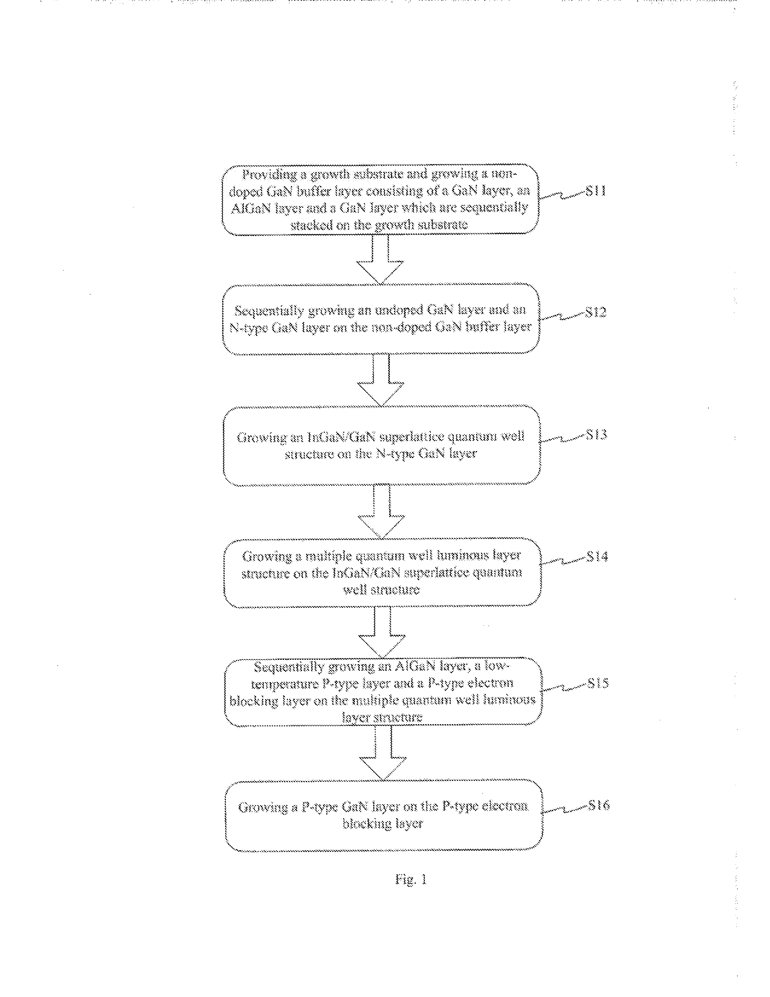
[0060]As shown in FIG. 1 to FIG. 7, this embodiment provides a preparation method of a GaN-based LED epitaxial structure, the preparation method comprises the following steps:
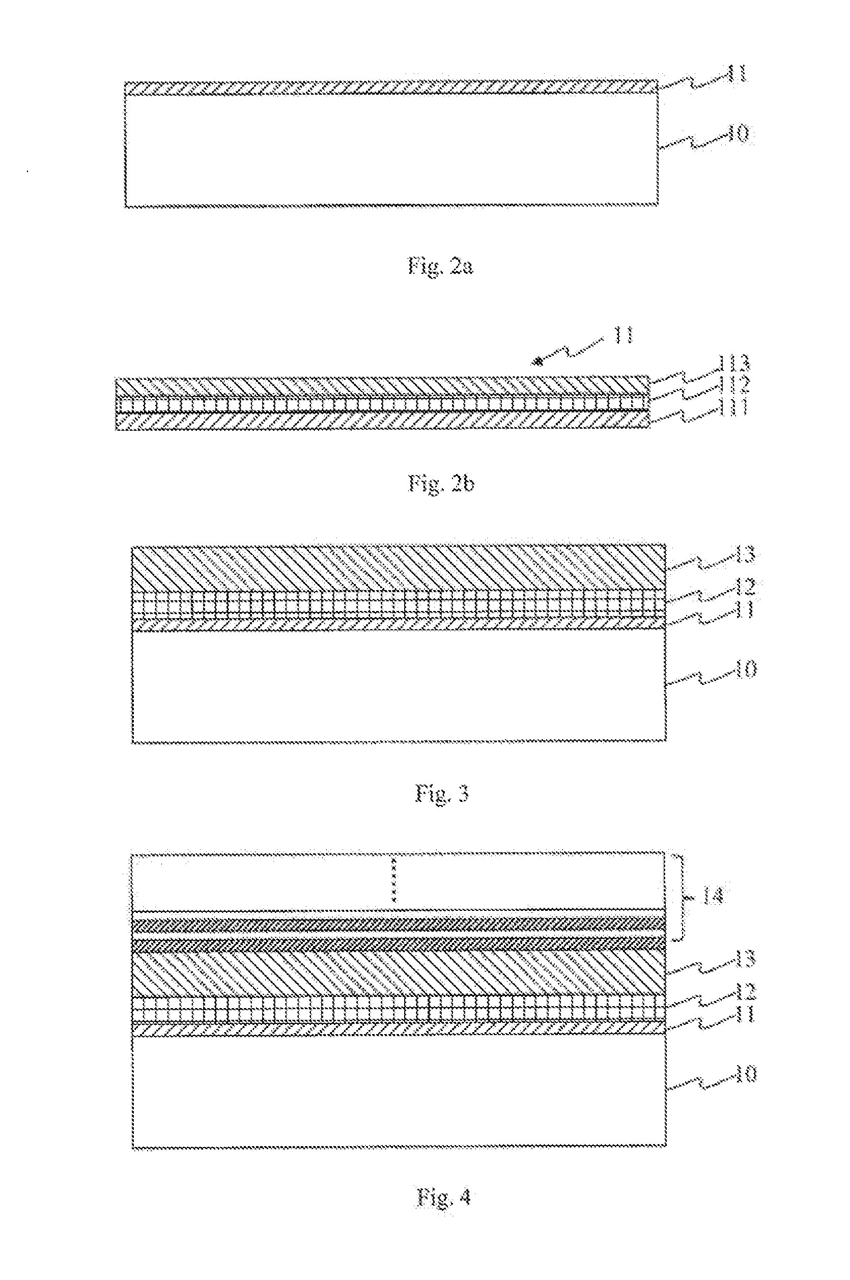
[0061]As shown in FIG. 1 and FIG. 2a to FIG. 2b, firstly perform step 1), i.e., S11: providing a growth substrate 10 and growing a non-doped GaN buffer layer 11 consisting of a GaN layer 111, an AlGaN layer 112 and a GaN layer 113 which are sequentially stacked on the growth substrate 10.
[0062]As an example, the growth substrate 10 can be sapphire, GaN, silicon, silicon carbide and the like. In this embodiment, the growth substrate 10 is a sapphire substrate.
[0063]As an example, growth temperature of the non-doped GaN buffer layer is comparatively low, a range of the growth temperature is 450-650° C. and a total growth thickness range is 15-50 nm. In this embodiment, the growth temperature of the non-doped GaN buffer layer is 400° C. and the total growth thickness is 30 nm.
[0064]As an example, the thickness of ...
embodiment 2
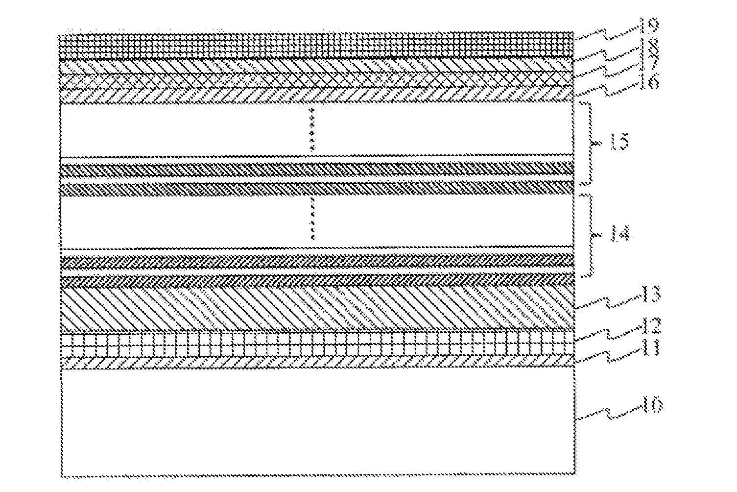
[0086]As shown in FIG. 7, this embodiment provides a GaN-based LED epitaxial structure. The epitaxial structure comprises a non-doped GaN buffer layer 11, an undoped GaN layer 12, an N-type GaN layer 13, an InGaN / GaN superlattice quantum well structure 14, a multiple quantum well luminous layer structure 15, an AlGaN layer 16, a low-temperature P-type layer 17, a P-type electron blocking layer 18 and a P-type GaN layer 19 which are sequentially stacked, wherein the non-doped GaN buffer layer 11 comprises a sandwich structure consisting of a GaN layer 111, an AlGaN layer 112 and a GaN layer 113 which are sequentially stacked.
[0087]As shown in FIG. 7, the GaN-based LED epitaxial structure is formed on a growth substrate 10 comprising one of sapphire, GaN, silicon and silicon carbide. In this embodiment, the GaN-based LED epitaxial structure is formed on a sapphire substrate.
[0088]As shown in FIG. 7, a total thickness range of the non-doped GaN buffer layer is 15-50 nm. In this embodim...
PUM
 Abstract
Description
Claims
Application Information


