Energy ray detector

Active Publication Date: 2016-10-27
SHARP KK
View PDF2 Cites 13 Cited by
  • Summary
  • Abstract
  • Description
  • Claims
  • Application Information

AI Technical Summary

Benefits of technology

[0039]According to one aspect of the present invention, information regarding energy ray radiation is detected from changes in an electrical property of the semiconductors which are arranged in a grid pattern and in which the electrical property changes in accordance with the amounts of applied energy ray radiation. Accordingly, the semiconductors need not have a thicker film thickness unlike the case in PTL 1 and PTL 2 where electric charges generated within the semiconductor film in response to application of radiation (energy ray radiation) to the semiconductor film are stored in the charge storage capacitors, and the stored electric charges are extracted to thereby detect the radiation. As a consequence, the semiconductors and the entire device can be made thinner.
[0040]Since the semiconductors can be made thinner, the problem does not arise in which a large internal stress is accumulated in the vicinity of the boundary between the area in which the semiconductor layer is formed and the area in which the semiconductor layer is not formed due to the difference in the amount of hardening shrinkage in the thickness, which may result in the lack of reliability, such as warps and lower impact-resistance.
[0041]In the case where electric charges generated within

Problems solved by technology

However, in the scintillation detection device, it is necessary to once convert incident energy rays into light and thereafter convert the light into elect

Method used


Image

  • Energy ray detector
  • Energy ray detector
  • Energy ray detector

Examples


first embodiment

[0095]One embodiment of the present invention is described below with reference to FIGS. 1(a) and 1(b) to FIG. 8.

[0096]1>

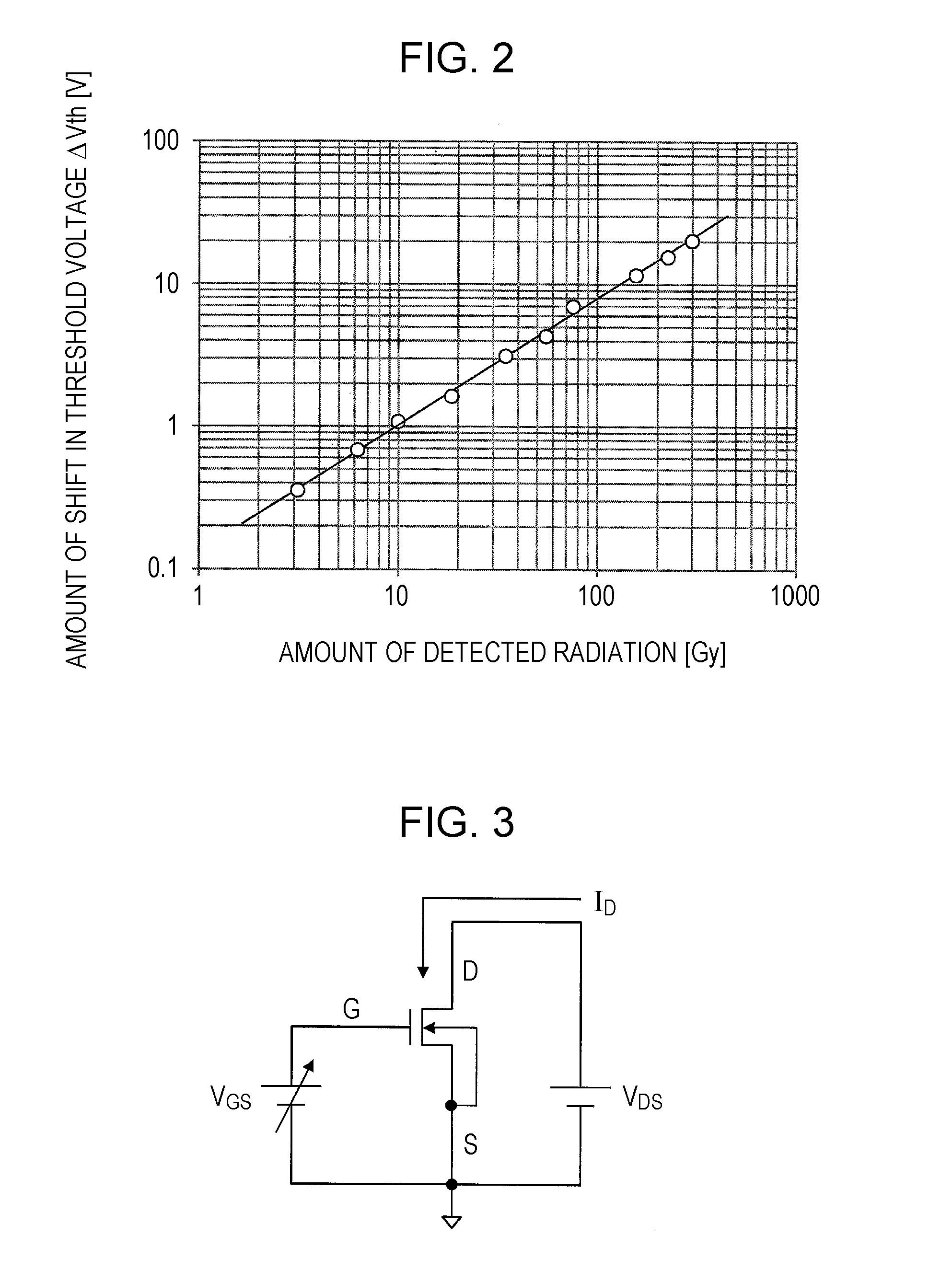
[0097]First, an example of the overall configuration of an energy ray detector according to the this embodiment using a TFT as the transistor illustrated in FIG. 3 having the gate voltage-drain current property illustrated in FIG. 5 is described.

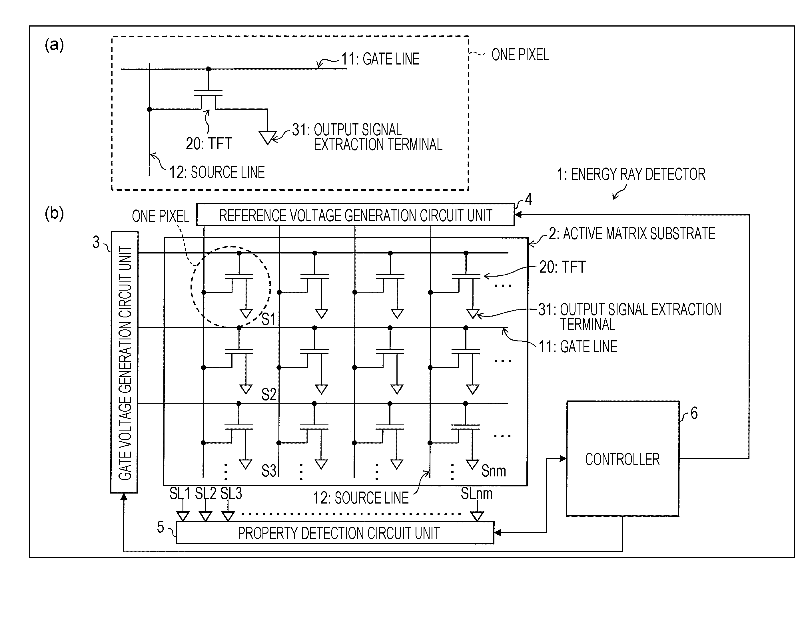
[0098]FIG. 1(a) is a circuit diagram illustrating a basic circuit configuration of one pixel in an energy ray detector 1 according to this embodiment, and FIG. 1(b) is a block diagram illustrating an example of the overall configuration of the energy ray detector 1 according to this embodiment.

[0099]As illustrated in FIG. 1(b), the energy ray detector 1 according to this embodiment includes an active matrix substrate 2, a gate voltage generation circuit unit 3 and a reference voltage generation circuit unit 4 that function as a drive circuit, a property detection circuit unit 5, and a controller 6.

[0100]These constituent e...

second embodiment

[0204]Another embodiment of the present invention is described below with reference to FIGS. 9(a) and 9(b). In this embodiment, differences from the first embodiment are described. Constituent elements having the same functions as the constituent elements used in the first embodiment are given the same reference numerals, and description thereof is omitted.

[0205]Also in this embodiment, the basic idea and the principle of energy ray detection in terms of the overview of the invention are the same as in the first embodiment.

[0206]In the first embodiment, the case is described, for example, where the radiation dose is detected from the electric current that increases when the TFT 20 of each pixel Sx is turned on. In this embodiment, a case is described, for example, where the radiation dose is detected from the electric current that increases when the TFT 20 that has been turned off transitions to the on state in accordance with a change in the threshold in response to application of ...

third embodiment

[0233]Yet another embodiment of the present invention is described below with reference to FIGS. 10(a) and 10(b). Here, differences between this embodiment and the first and second embodiments are described. Constituent elements having the same functions as the constituent elements used in the first and second embodiments are given the same reference numerals, and description thereof is omitted.

[0234]In a capacitor element formed by using a transistor that has an active layer formed of a semiconductor, when radiation is applied to the capacitor element, the capacitance value linearly transitions in accordance with the amount of applied radiation.

[0235]Therefore, by detecting, as the amount of change in an electrical property of the semiconductor, the amount of change (amount of transition) in the capacitance value of the capacitor element formed by using the transistor having an active layer formed of a semiconductor, the radiation dose can be determined from the amount of change in...


PUM


Abstract

A thin, lightweight, and highly reliable energy ray detector that enables high-speed reading is provided. An energy ray detector (1) includes TFTs (20) that are arranged in a grid pattern and that each have an active layer formed of a semiconductor having an electrical property changing in accordance with the amount of applied energy ray radiation, and a property detection circuit unit (5) and a controller (60) that detect information regarding the energy ray radiation from changes in the electrical property of the TFTs (20).

Description

TECHNICAL FIELD[0001]The present invention relates to an energy ray detector including semiconductors arranged in a grid pattern to detect energy ray radiation from changes in an electrical property of the semiconductors.BACKGROUND ART[0002]As energy ray detection devices that detect energy rays (radiation), such as X-rays, two major types of detection devices are known. One is a scintillation detection device that employs an indirect conversion scheme in which energy rays are converted into light with a scintillator, and the light is converted into electric signals with a photoelectric transducer, such as a photodiode. The other is a semiconductor detection device that employs a direct conversion scheme in which energy rays are directly converted into electric charges with a semiconductor layer.[0003]However, in the scintillation detection device, it is necessary to once convert incident energy rays into light and thereafter convert the light into electric signals with a photoelect...

Claims


Application Information

Patent Timeline
IPC IPC(8): G01T1/24
CPCG01T1/247H01L27/14612H01L27/14658
Inventor MASUDA, RYOHICHIKATAYAMA, MIKIOKAWANISHI, HIDENORI
Owner SHARP KK
Why Eureka
Try Eureka