Method for manufacturing resistive element, method for manufacturing pressure sensor element, pressure sensor element, pressure sensor, altimeter, electronic apparatus, and moving object

Active Publication Date: 2016-12-01
SEIKO EPSON CORP
View PDF7 Cites 4 Cited by
  • Summary
  • Abstract
  • Description
  • Claims
  • Application Information

AI Technical Summary

Benefits of technology

[0039]According to the moving object, the miniaturization and

Problems solved by technology

However, in the method disclosed in JP-A-7-131035, since the resistive layer is formed to a relatively deep position, when, for example, the resistive element is used to detect the deflection of

Method used


Image

  • Method for manufacturing resistive element, method for manufacturing pressure sensor element, pressure sensor element, pressure sensor, altimeter, electronic apparatus, and moving object
  • Method for manufacturing resistive element, method for manufacturing pressure sensor element, pressure sensor element, pressure sensor, altimeter, electronic apparatus, and moving object
  • Method for manufacturing resistive element, method for manufacturing pressure sensor element, pressure sensor element, pressure sensor, altimeter, electronic apparatus, and moving object

Examples


first embodiment

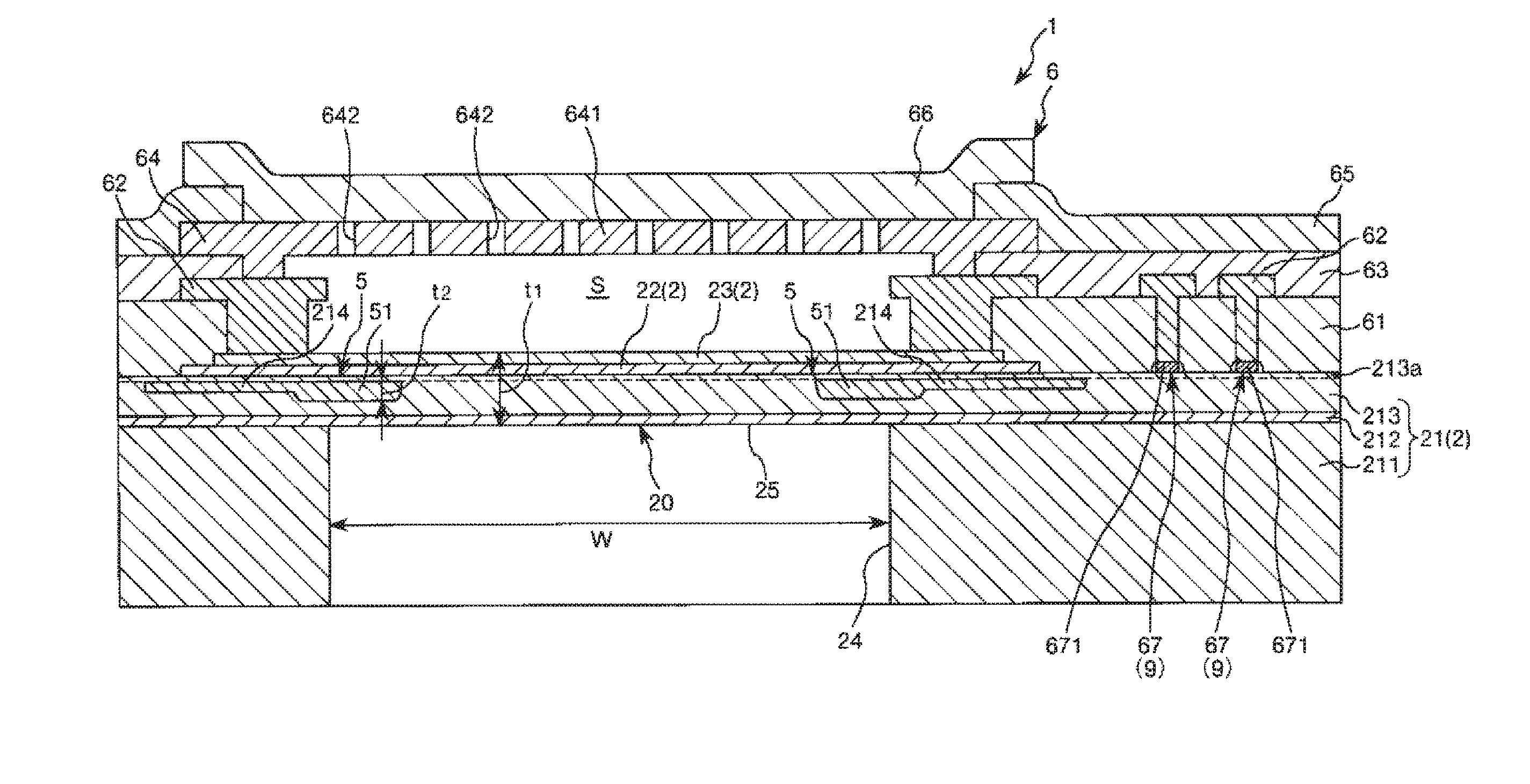
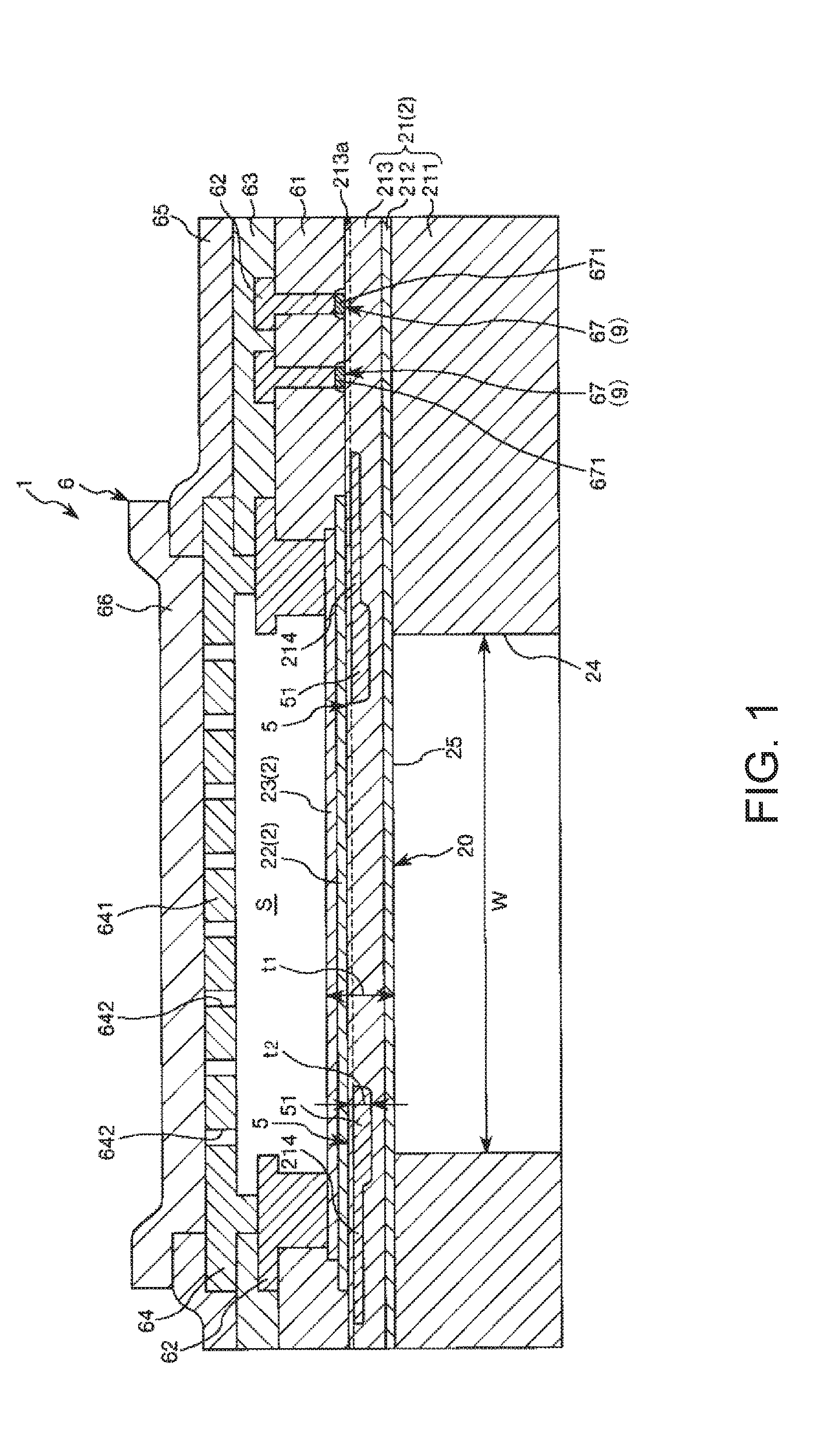
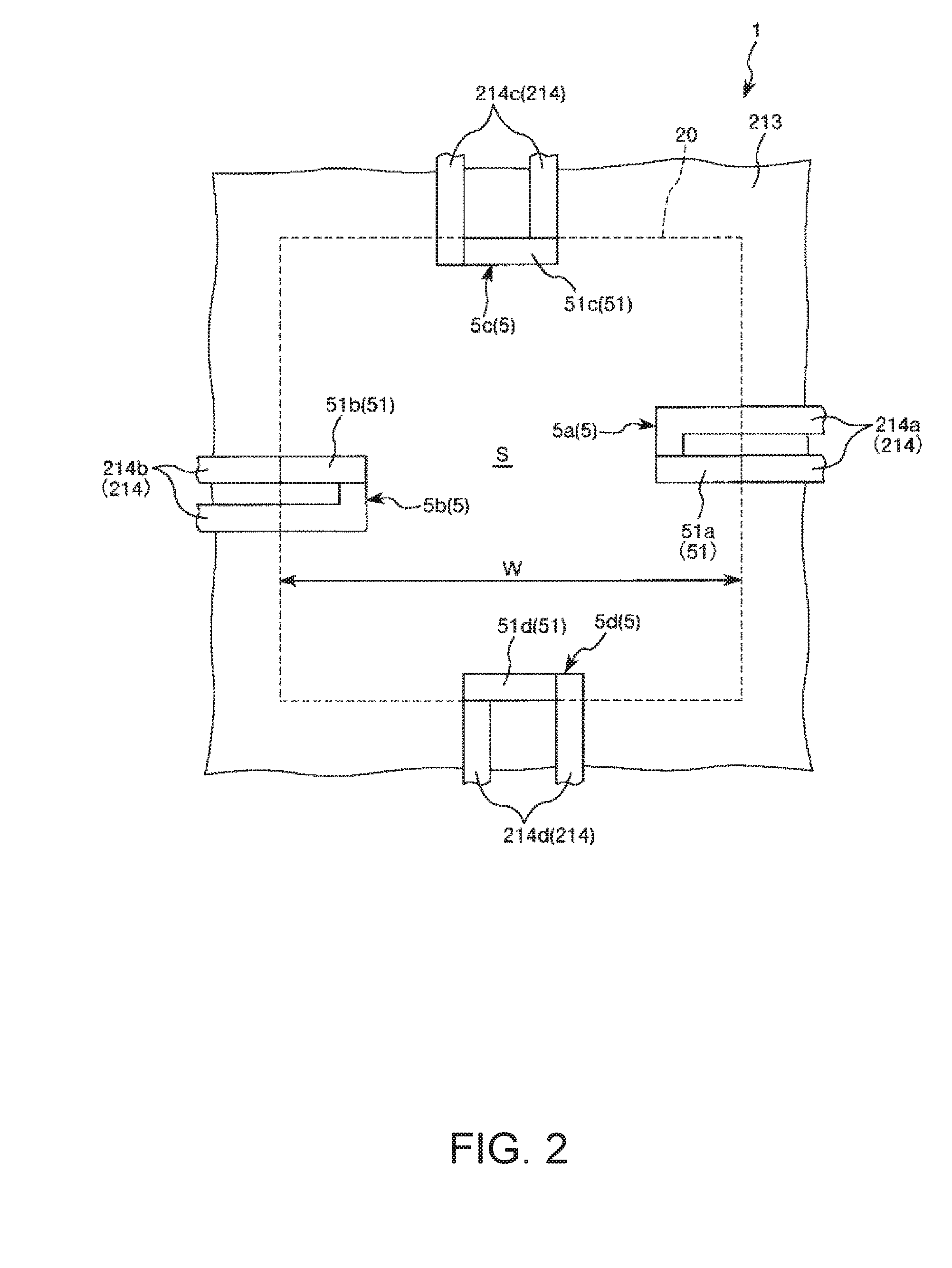
[0055]FIG. 1 is a cross-sectional view showing a pressure sensor element according to a first embodiment of the invention. FIG. 2 is a plan view showing the arrangement of resistive elements included in the pressure sensor element shown in FIG. 1. FIG. 3 is a graph showing an example of a carrier concentration distribution of a resistive region of the resistive element shown in FIG. 2. FIGS. 4A and 4B are diagrams for explaining the operation of the pressure sensor element shown in FIG. 1, in which FIG. 4A is a cross-sectional view showing a pressurized state and FIG. 4B is a plan view showing the pressurized state. In the following, the upper side in FIG. 1 is defined as “top”, while the lower side is defined as “bottom”, for convenience of description.

[0056]The pressure sensor element 1 shown in FIG. 1 includes a substrate 2 including a diaphragm portion 20, a plurality of piezoresistive elements 5 (resistive elements) provided in the diaphragm portion 20, a stacked structure 6 fo...

second embodiment

[0139]FIG. 9 is a cross-sectional view showing a pressure sensor element according to a second embodiment of the invention.

[0140]The pressure sensor element of the embodiment is similar to that of the first embodiment except that the configuration (arrangement) of the pressure reference chamber is different.

[0141]In the following description, the second embodiment will be described mainly on differences from the embodiment described above, and a description of similar matters is omitted. Moreover, in FIG. 9, configurations similar to those of the embodiment described above are denoted by the same reference and numeral signs.

[0142]The pressure sensor element 1A shown in FIG. 9 includes, instead of the stacked structure 6 of the first embodiment, a substrate 3 forming a cavity S1 (pressure reference chamber) together with the substrate 2. Here, the substrate 3 closes the opening of the recess 24 of the substrate 2 and is bonded to the lower surface (surface of the silicon layer 211) o...


PUM

PropertyMeasurementUnit
Lengthaaaaaaaaaa
Fractionaaaaaaaaaa
Fractionaaaaaaaaaa

Abstract

A method for manufacturing a resistive element includes: preparing a substrate including an n-type silicon layer; doping the silicon layer with an impurity to thereby form a resistive region; heat-treating the resistive region by any of rapid thermal annealing, flash lamp annealing, and excimer laser annealing; and epitaxially growing silicon on the resistive region to thereby form a covering layer.

Description

CROSS REFERENCE[0001]This application claims benefits of Japanese Application JP 2015-109533, filed on May 29, 2015 and Japanese Application JP2016-102803, filed on May 23, 2016. The disclosures of the prior applications are hereby incorporated by reference herein in their entirety.BACKGROUND[0002]1. Technical Field[0003]The present invention relates to a method for manufacturing a resistive element, a method for manufacturing a pressure sensor element, a pressure sensor element, a pressure sensor, an altimeter, an electronic apparatus, and a moving object.[0004]2. Related Art[0005]In microelectromechanical systems (MEMS) (especially a sensor device), forming a resistive element (piezoresistive element) by doping single-crystal silicon with an impurity has been widely performed.[0006]As a method for manufacturing the resistive element, for example, a method in which boron is implanted into an n-type silicon substrate while being accelerated to an energy of 1 MeV to thereby form a p-...

Claims


Application Information

Patent Timeline
IPC IPC(8): B81B3/00B81C1/00
CPCB81B3/0045B81C2201/0116B81B2201/0264B81C1/00158G01L9/0042G01L9/0054H01L29/84H01L28/20H01L21/02532H01L21/26513H01L21/02634B81B2207/07B81B2203/0127
Inventor SHIMADA, HIROYUKI
Owner SEIKO EPSON CORP
Why Eureka
Try Eureka