Photoelectric conversion element and imaging device

a conversion element and imaging device technology, applied in the direction of electrical equipment, semiconductor devices, radio control devices, etc., can solve the problems of difficult imaging, low illumination condition, and cost of achieving 4k/8k broadcasting, and achieve low illumination condition, easy imaging, and excellent imaging performance.

Active Publication Date: 2017-01-05
SEMICON ENERGY LAB CO LTD
View PDF4 Cites 13 Cited by
  • Summary
  • Abstract
  • Description
  • Claims
  • Application Information

AI Technical Summary

Benefits of technology

[0016]In view of the above, an object of one embodiment of the present invention is to provide an imaging device with excellent imaging performance. Another object is to provide an imaging device that easily performs imaging under a low illuminance condition. Another object is to provide a low power consumption imaging device. Another object is to provide an imaging device that is suitable for high-speed operation. Another object is to provide a high resolution imaging device. Another object is to provide an imaging device with little noise. Another object is to provide an imaging device with a high S / N ratio. Another object is to provide an imaging device with small variations in characteristics between its pixels. Another object is to provide a highly integrated imaging device. Another object is to provide an imaging device which can be used in a wide temperature range. Another object is to provide an imaging device with a high aperture ratio. Another object is to provide an imaging device with high reliability. Another object is to provide a novel imaging device or the like. Another object is to provide a novel semiconductor device or the like.

Problems solved by technology

Note that there are many challenges to be solved such as technology and cost for achieving 4K / 8K broadcasting.
When the light-receiving area of the photoelectric conversion element is reduced, it might be difficult to perform imaging under a low illuminance condition because of the decrease in sensitivity to light.
However, such a photoelectric conversion element has a relatively large dark current, which might cause deterioration in imaging quality.
One of the factors in the dark current is thought to be insufficient suppression of charge injection into the chalcopyrite semiconductor from an electrode.
The hole injection blocking layer is effective in suppressing a dark current; however, a hole injection blocking layer whose material has a low electrical conductivity or a thick hole injection blocking layer degrades the performance of the imaging device.
Note that the above problems arise not necessarily only when an imaging device includes pixels of high resolution such as 8K, but also when an imaging device includes pixels of 4K resolution or lower.

Method used


Image

  • Photoelectric conversion element and imaging device
  • Photoelectric conversion element and imaging device
  • Photoelectric conversion element and imaging device

Examples


embodiment 1

[0056]In this embodiment, a photoelectric conversion element 100 of one embodiment of the present invention will be described with reference to drawings.

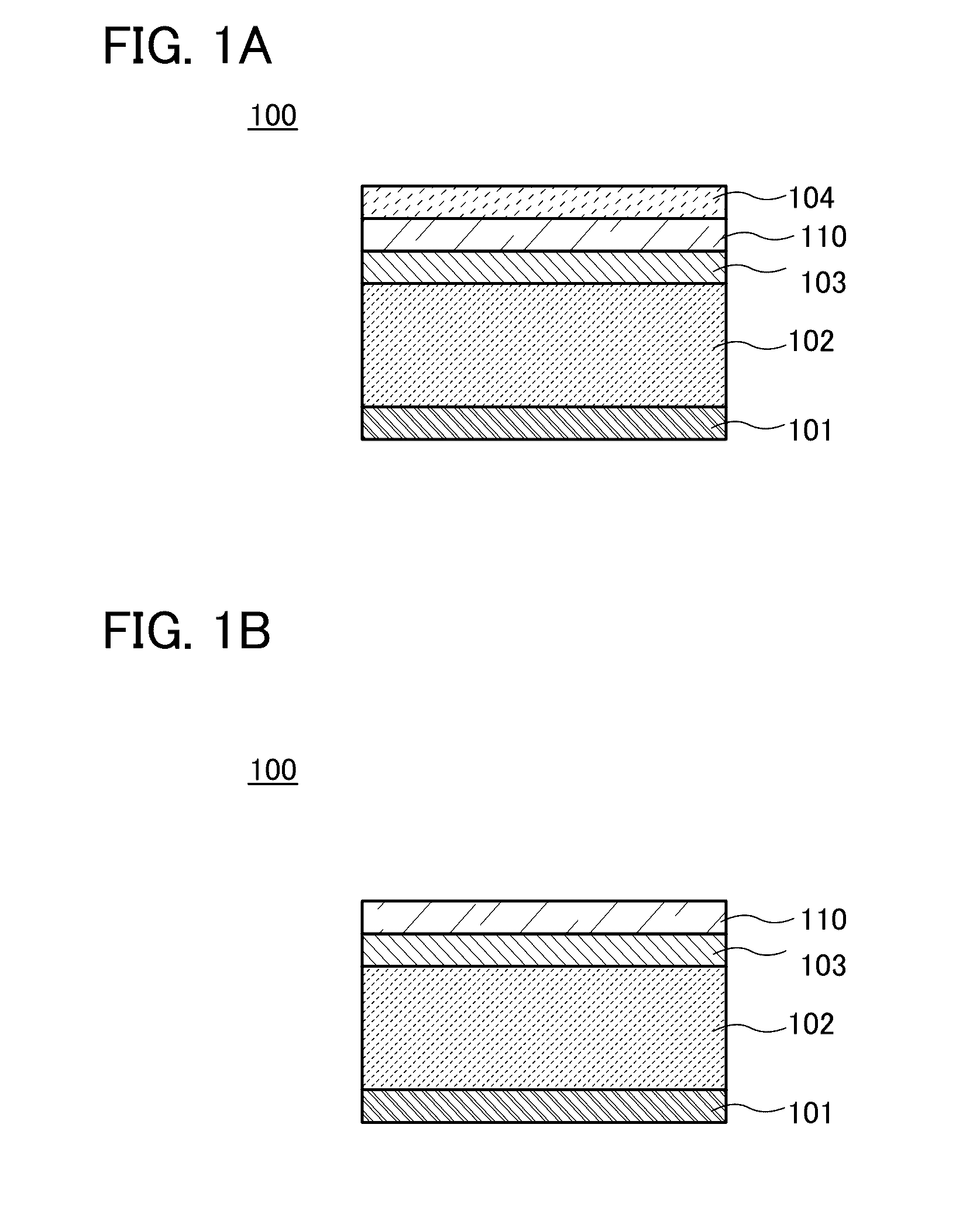
[0057]FIG. 1A schematically illustrates a cross-sectional structure of the photoelectric conversion element 100 of one embodiment of the present invention. The photoelectric conversion element 100 includes a first electrode 101, a photoelectric conversion layer 102 over the first electrode 101, a hole injection blocking layer 103 over the photoelectric conversion layer 102, an oxide layer 110 over the hole injection blocking layer 103, and a second electrode 104 over the oxide layer 110.

[0058]The photoelectric conversion element 100 may be formed over a substrate or over a driver transistor which is formed in a substrate or formed over a substrate.

[0059]FIG. 1B schematically illustrates a cross-sectional structure of the photoelectric conversion element 100 of one embodiment of the present invention. The photoelectric conversion ele...

embodiment 2

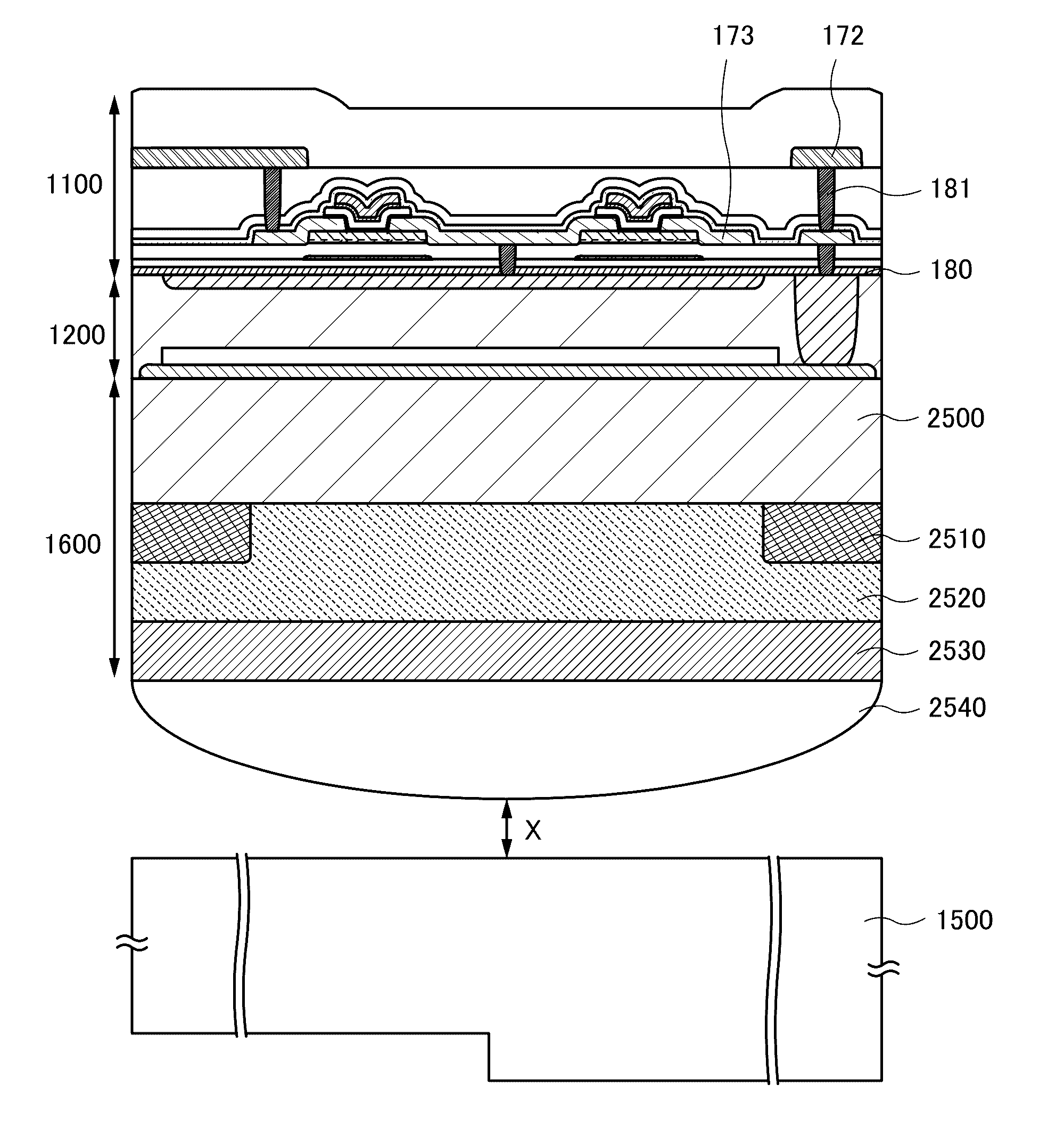
[0110]Next, specific structure examples of an imaging device of one embodiment of the present invention will be described with reference to drawings. FIG. 3A is an example of a cross-sectional view of an imaging device of one embodiment of the present invention and illustrates an example of specific connection between the photoelectric conversion element 100 in FIG. 1A and driver transistors. The imaging device includes a layer 1100 including a transistor 151 and a transistor 152 and a layer 1200 including the photoelectric conversion element 100.

[0111]Although the wirings, the electrodes, and the conductors are illustrated as independent components in cross-sectional views in this embodiment, some of them are provided as one component in some cases when they are electrically connected to each other. In addition, a structure in which a gate electrode, a source electrode, or a drain electrode of the transistor is connected to the wirings through the conductor is only an example, and ...

embodiment 3

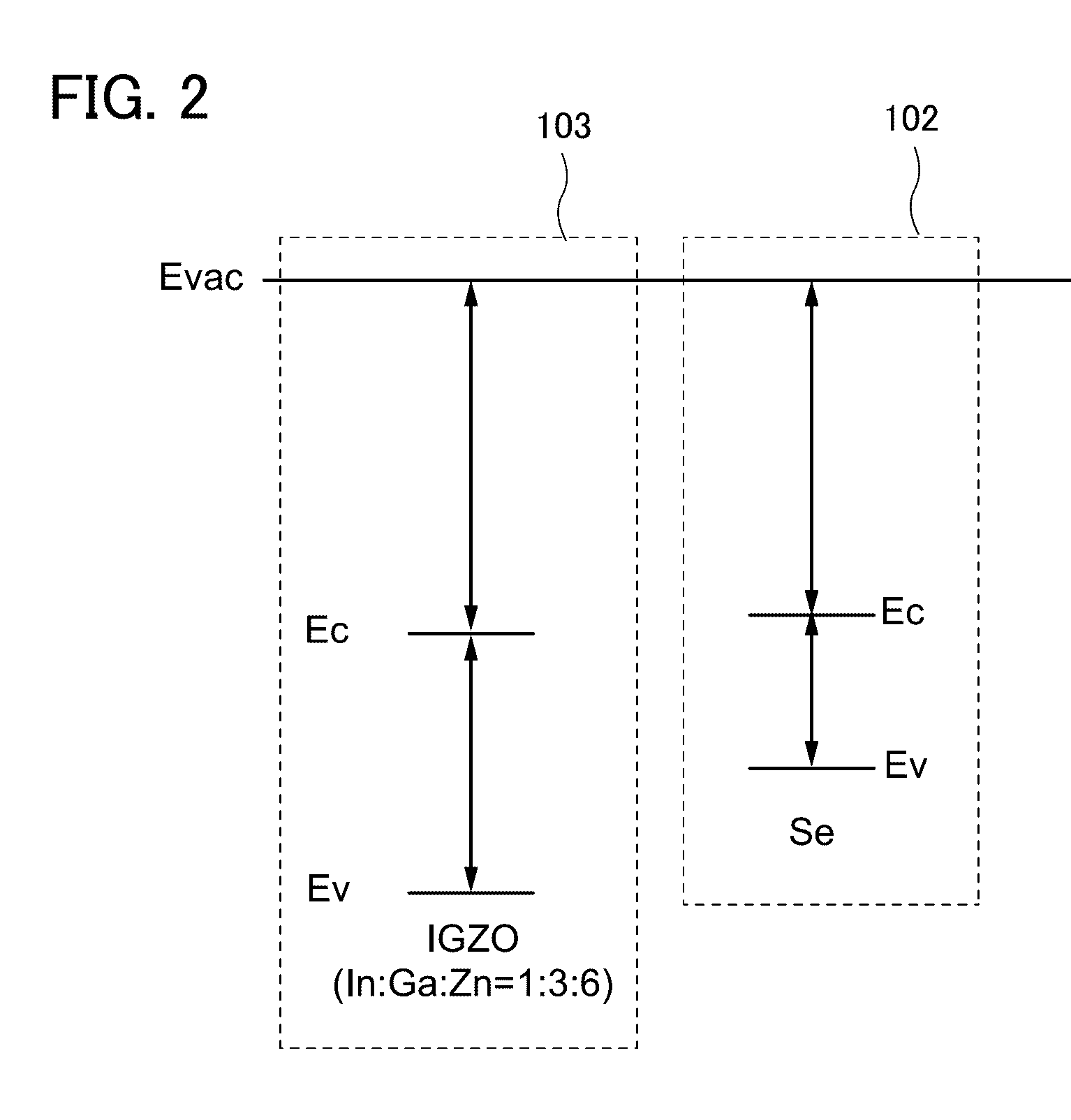
[0175]In an imaging device of one embodiment of the present invention, an oxide as typified by an In—Ga—Zn oxide is used for the hole injection blocking layer included in the photoelectric conversion element. In this embodiment, the oxide will be described. Note that the oxide can be used as a semiconductor also for a transistor which is connected to the photoelectric conversion element; thus, its effective properties when the oxide is used for a transistor will also be described.

[0176]A structure of the oxide is described below.

[0177]An oxide is classified into a single crystal oxide and the other, a non-single-crystal oxide. Examples of the non-single-crystal oxide include an oxide having a c-axis-aligned crystalline (CAAC) structure, a polycrystalline oxide, an oxide having a nanocrystalline (nc) structure, an amorphous-like (a-like) oxide, and an amorphous oxide.

[0178]From another perspective, an oxide is classified into an amorphous oxide and the other, a crystalline oxide. Exa...


PUM


Abstract

An imaging device with excellent imaging performance is provided. An imaging device that easily performs imaging under a low illuminance condition is provided. A low power consumption imaging device is provided. An imaging device with small variations in characteristics between its pixels is provided. A highly integrated imaging device is provided. A photoelectric conversion element includes a first electrode, and a first layer, a second layer, and a third layer. The first layer is provided between the first electrode and the third layer. The second layer is provided between the first layer and the third layer. The first layer contains selenium. The second layer contains a metal oxide. The third layer contains a metal oxide and also contains at least one of a rare gas atom, phosphorus, and boron. The selenium may be crystalline selenium. The second layer may be a layer of an In—Ga—Zn oxide including c-axis-aligned crystals.

Description

BACKGROUND OF THE INVENTION[0001]1. Field of the Invention[0002]One embodiment of the present invention relates to a photoelectric conversion element and an imaging device.[0003]Note that one embodiment of the present invention is not limited to the above technical field. The technical field of one embodiment of the invention disclosed in this specification and the like relates to an object, a method, or a manufacturing method. In addition, one embodiment of the present invention relates to a process, a machine, manufacture, or a composition of matter. Specifically, examples of the technical field of one embodiment of the present invention disclosed in this specification include a semiconductor device, a display device, a liquid crystal display device, a light-emitting device, a lighting device, a power storage device, a storage device, an imaging device, a method for driving any of them, and a method for manufacturing any of them.[0004]In this specification and the like, a semicond...

Claims


Application Information

Patent Timeline
Patent Type & Authority Applications(United States)
IPC IPC(8): H01L27/146H01L31/109H01L31/0296H01L31/0224H01L31/0272
CPCH01L27/14647H01L27/14665H01L27/14694H01L27/14696H01L31/032H01L27/14607H01L27/14636H01L27/14627H01L27/14621H01L27/14612H01L31/0272H01L31/109H01L31/0224H01L31/022475H01L31/0296
Inventor YAMAZAKI, SHUNPEINONAKA, YUSUKEKATAISHI, RIHOOHKI, HIROSHISATO, YUICHIMATSUBAYASHI, DAISUKE
Owner SEMICON ENERGY LAB CO LTD
Why Eureka
Try Eureka