Device and method to connect gate regions separated using a gate cut

Inactive Publication Date: 2017-01-19
QUALCOMM INC
View PDF6 Cites 29 Cited by
  • Summary
  • Abstract
  • Description
  • Claims
  • Application Information

AI Technical Summary

Benefits of technology

[0004]A fabrication process may include forming a gate line of a device, such as gate line used to create gate terminals of one or more fin field-effect-transistor (finFET) devices. The fabrication process may also include cutting the gate line to define a first gate region and a second gate region and forming a conductive structure to connect the first gate region and the second gate region (e.g., to “reconnect” the gate line). Cutting the gate line may “distribute” strain associated with one or more neighboring devices, such as dummy finFET devices formed by cutting an adjacent gate line and filling in a dielectric between the dummy finFET devices. Focusing of strain on the device may be reduced or avo

Problems solved by technology

In some circumstances, devices nearer to a cut may operate differently as compared to devices farther from the cut (i.e., the devices may be “mismatched”).
Thus, performance of a device can deviate from a design specification of the device depending on the particular physical layout used to fabricate the device, which may reduce device performance or cause device malfunction.
This technique may reduce circuit performance (e.g., due to a greater amount of wiring to connect devices) and may increase circuit area in some cases.
This techn

Method used


Image

  • Device and method to connect gate regions separated using a gate cut
  • Device and method to connect gate regions separated using a gate cut
  • Device and method to connect gate regions separated using a gate cut

Examples


Embodiment Construction

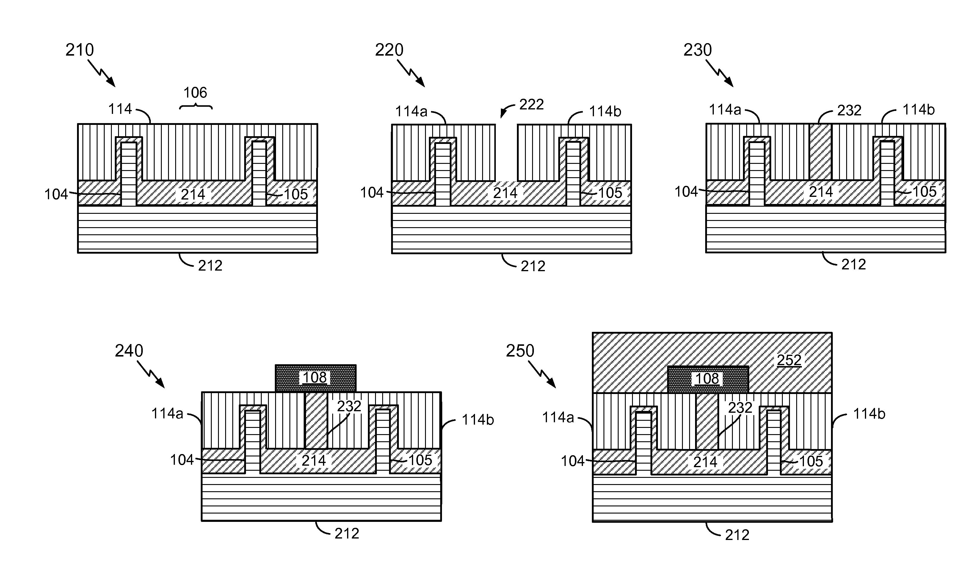
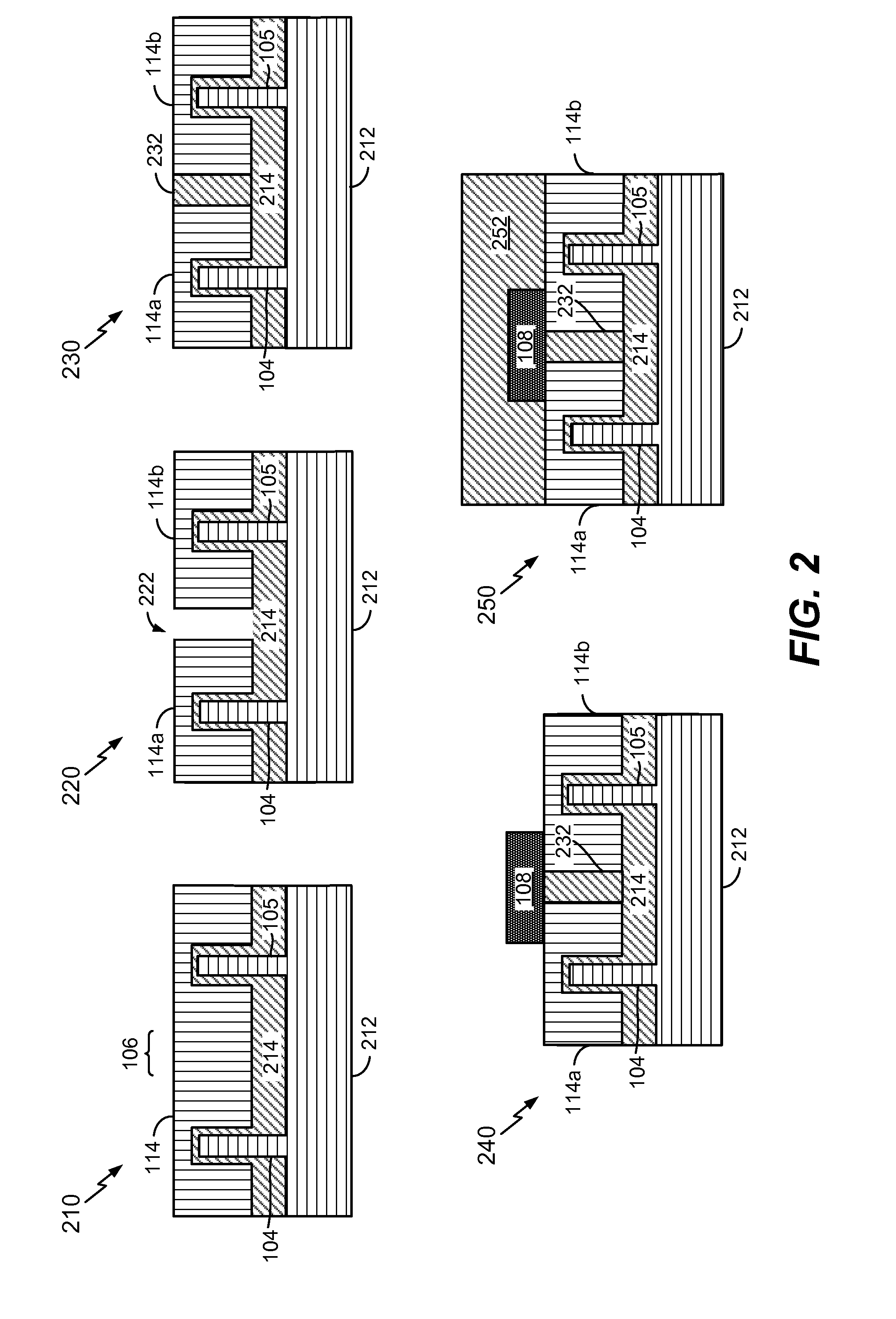
[0018]Certain examples are described below with reference to the drawings. In the description and the drawings, similar or common features may be indicated by common reference numbers.

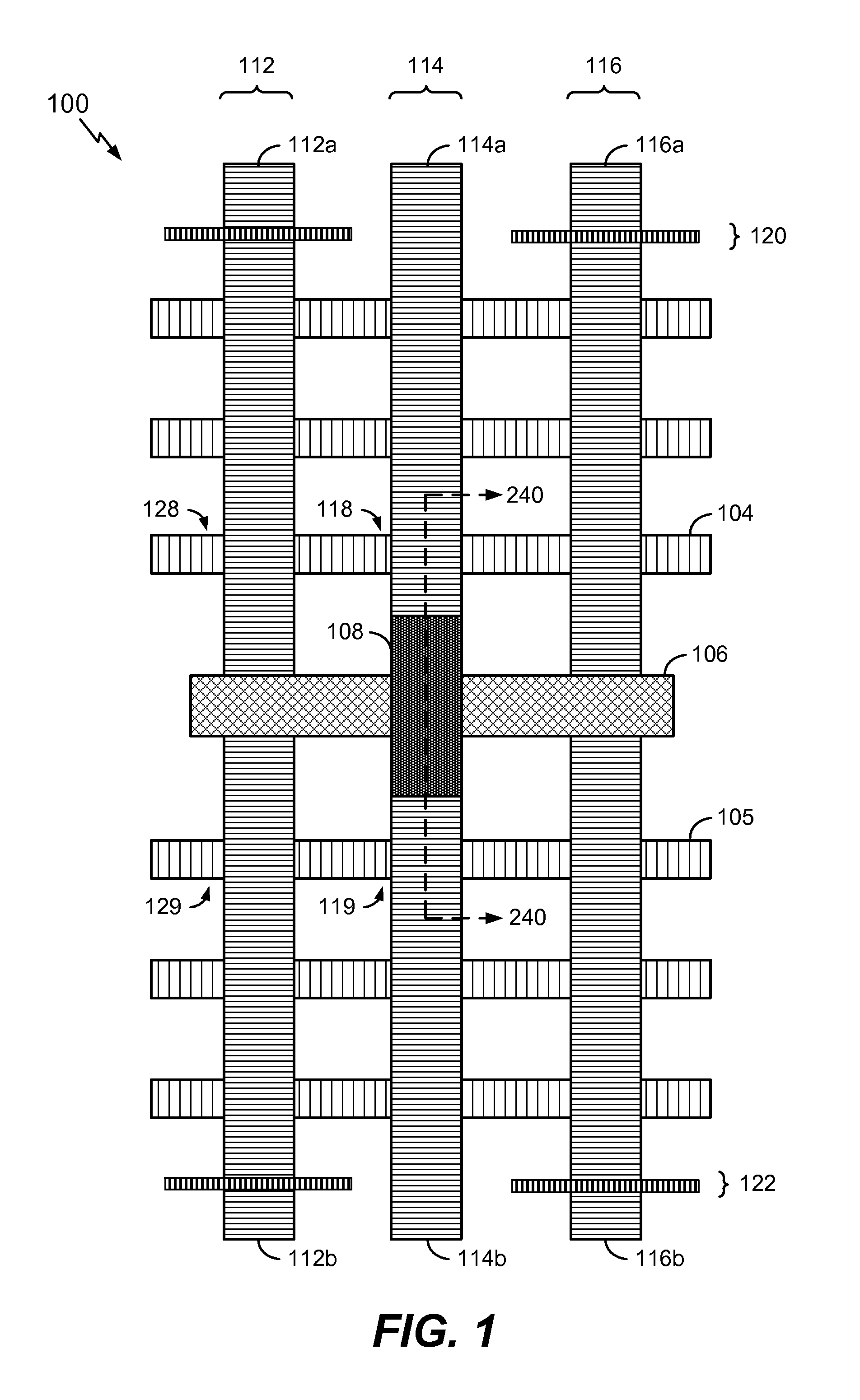
[0019]FIG. 1 depicts a layout view of an illustrative example of a device 100. The device 100 includes multiple gate lines, such as a first gate line 114 (e.g., a structure used to form multiple transistor gate regions). The device 100 may also include a second gate line 112 and a third gate line 116. The gates lines 112, 114, and 116 may include polycrystalline silicon (polysilicon or poly-Si) or metal, such as titanium nitride (TiN), tungsten (W), aluminum (Al), etc. The device 100 further includes multiple fins, such as a fin 104 and a fin 105. For example, the fins 105, 104 may be defined from a substrate (e.g., a silicon substrate) of the device 100 by etching the substrate.

[0020]Multiple devices (e.g., transistors) may be formed using a single gate line of the device 100. For example, two transis...


PUM


Abstract

A method of fabrication of a device includes performing a gate cut to cut a gate line to create a first gate region and a second gate region. The method further includes depositing a conductive material to form a conductive jumper structure to connect the first gate region and the second gate region.

Description

I. FIELD[0001]This disclosure is generally related to electronic devices and more particularly to semiconductor devices.II. DESCRIPTION OF RELATED ART[0002]Certain semiconductor fabrication processes include forming a structure (e.g., polysilicon) and cutting the structure into multiple regions. In some circumstances, devices nearer to a cut may operate differently as compared to devices farther from the cut (i.e., the devices may be “mismatched”). Thus, performance of a device can deviate from a design specification of the device depending on the particular physical layout used to fabricate the device, which may reduce device performance or cause device malfunction.[0003]Some fabrication techniques may avoid cuts. For example, a layout of a circuit may be rearranged to avoid a cut. This technique may reduce circuit performance (e.g., due to a greater amount of wiring to connect devices) and may increase circuit area in some cases. Some fabrication techniques may attempt to “isolate...

Claims


Application Information

Patent Timeline
IPC IPC(8): H01L29/423H01L27/092H01L21/304H01L29/66G06F17/50H01L21/8238
CPCH01L29/4238G06F17/5077H01L21/823821H01L27/0924H01L21/823871H01L21/3043H01L29/6681H01L21/823828H01L27/0207H01L27/092G06F30/394H01L23/5386
Inventor LIU, YANXIANGSONG, STANLEY SEUNGCHULRIM, KERN
Owner QUALCOMM INC
Why Eureka
Try Eureka