Organic Light-Emitting Diode Device and Manufacturing Method Thereof and Organic Light-Emitting Display Panel

a technology of light-emitting diodes and manufacturing methods, applied in the field of display devices, can solve the problems of oled display screen display effects and display effects that will also decline, and achieve the effects of reducing manufacturing costs, reducing cathode thickness, and facilitating node adjustmen

Inactive Publication Date: 2017-01-26
EVERDISPLAY OPTRONICS (SHANGHAI) CO LTD
View PDF0 Cites 4 Cited by
  • Summary
  • Abstract
  • Description
  • Claims
  • Application Information

AI Technical Summary

Benefits of technology

[0008]In view of the deficiency of prior art, the technical solution of the invention provides an organic light-emitting diode device and a manufacturing method thereof and an organic light-emitting display panel. In the technical solution of the invention, a micro-cavity adjusting layer is spin-coated on a ca

Problems solved by technology

As a display device, the OLED display screen may also be affected by environmental factors; especia

Method used


Image

  • Organic Light-Emitting Diode Device and Manufacturing Method Thereof and Organic Light-Emitting Display Panel
  • Organic Light-Emitting Diode Device and Manufacturing Method Thereof and Organic Light-Emitting Display Panel
  • Organic Light-Emitting Diode Device and Manufacturing Method Thereof and Organic Light-Emitting Display Panel

Examples


embodiment 1

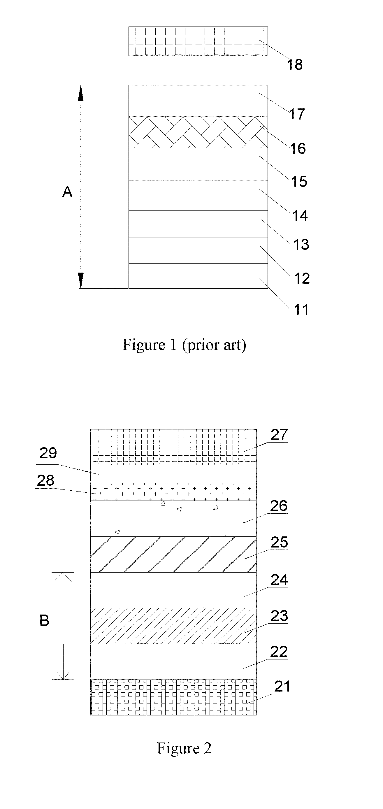
[0058]To solve the defects like the longer evaporation time, the extending length of the electric current passed through, the increasing resistance, and the reducing emitting efficiency of the OLED device caused by a thicker total thickness of evaporation of the micro-cavity adjusting layer in prior art, the invention provides a micro-cavity adjusting structure, specifically as shown in FIG. 2, the general scheme of which is to configure the micro-cavity adjusting layer, which traditionally needs to be evaporated, on the cover by spin-coating, to achieve the purpose of the technical solution of the invention.

[0059]As shown in FIG. 2, in the embodiment of the invention, the organic light-emitting diode device mainly comprises:

[0060]An anode layer 21; the anode layer is an ITO / Ag / ITO anode layer specifically in the embodiment of the invention; in this field, the anode layer 21 can also choose other metal with high reflectivity and high work function.

[0061]An OLED device layer (marked ...

embodiment 2

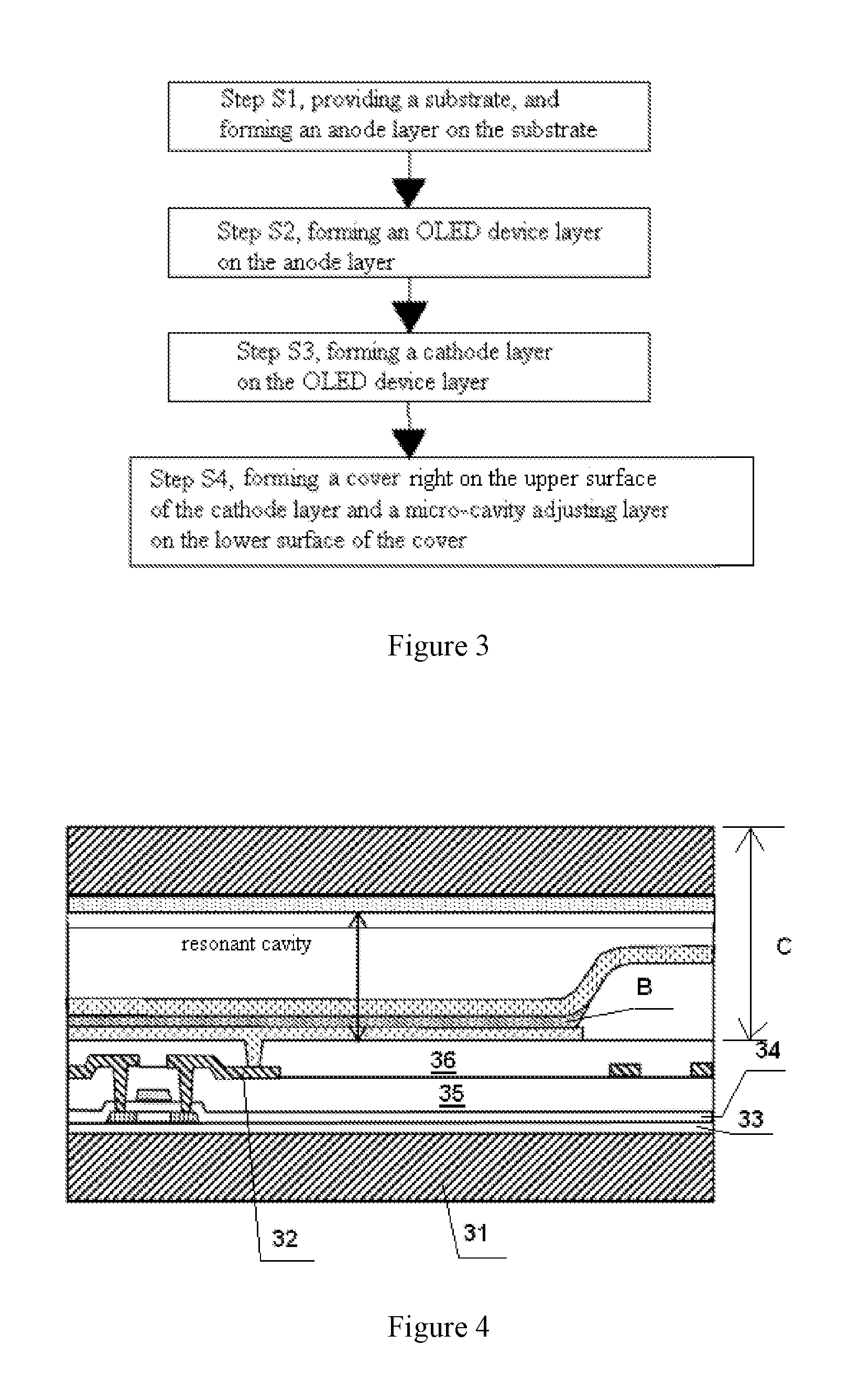
[0069]Based on the above-mentioned organic light-emitting diode device, the invention also provides the manufacturing method of the organic light-emitting diode device, specifically as the procedure diagram shown in FIG. 3.

[0070]Step S1, providing a substrate, and forming an anode layer on the substrate. In the embodiment of the invention, the anode layer specifically is an ITO anode layer; in this field, the anode layer can also be other metal with high reflectivity.

[0071]Step S2, forming an OLED device layer on the anode layer; as an emitting device, the OLED device layer mainly comprises a hole-transporting layer, an emitting layer and an electron-transporting layer, stacked in order from bottom to top; wherein the hole-transporting layer of the OLED device layer covers on the anode layer.

[0072]Step S3, forming a cathode layer on the upper surface of the OLED device layer; in the embodiment, the metal with higher transmittance is chose to be the cathode layer (i.e. the transparen...

embodiment 3

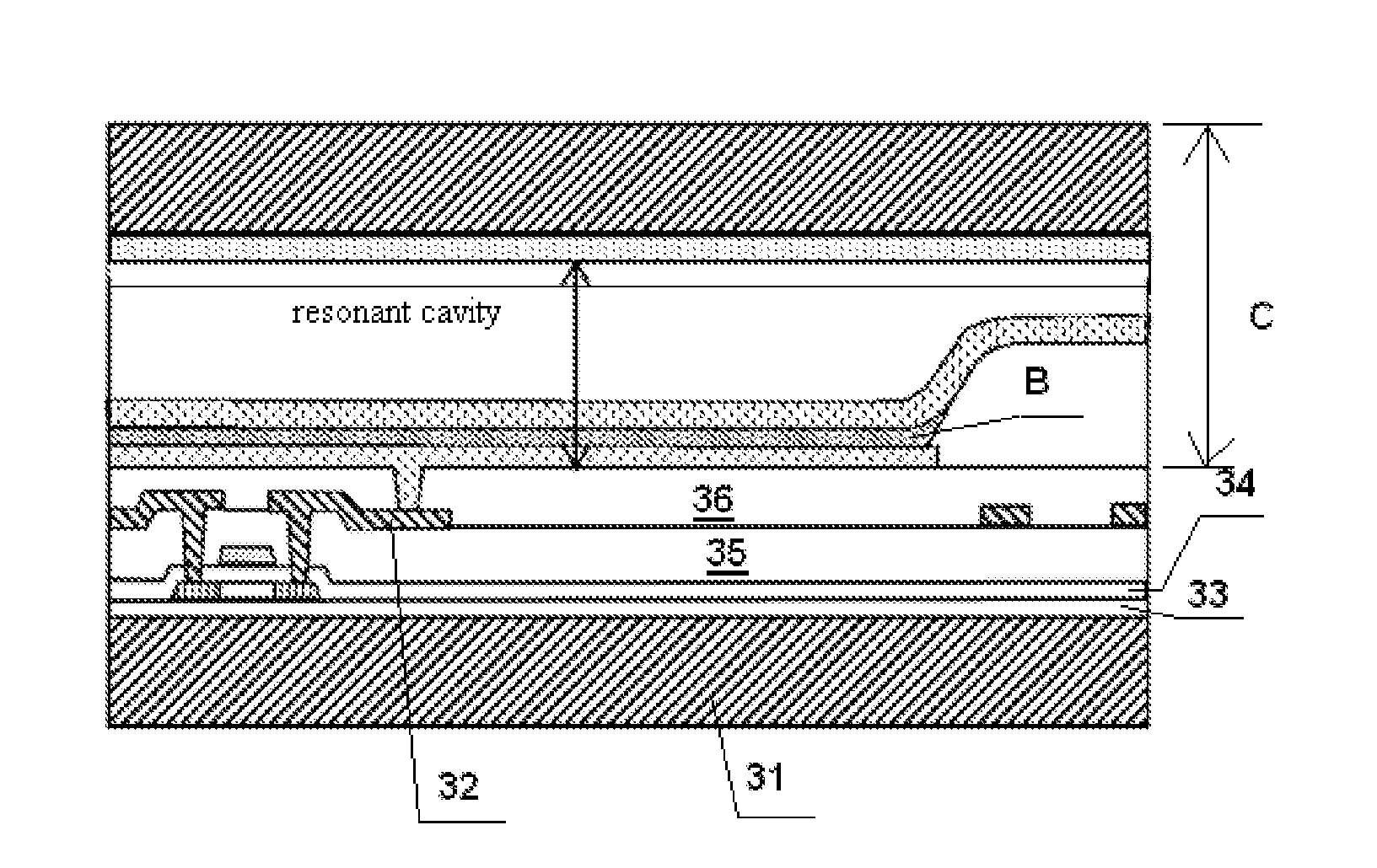
[0077]Based on the above-mentioned organic light-emitting diode device, the invention also provides an organic light-emitting display panel using the organic light-emitting diode device, and its structure shown in FIG. 4 comprises:

[0078]an array substrate 31; a buffer layer 33, covering on the array substrate 31; a gate insulating layer 34, covering on the buffer layer 33; an insulating layer 35, covering on the gate insulating layer 34; a planarizing layer 36, covering on the insulating layer 35.

[0079]In the gate insulating layer 34, the insulating layer 35 and the planarizing layer 36, there also provides a thin-film transistor 32 located above the array substrate 31.

[0080]The organic light-emitting diode device (marked C in the Figure) described in Embodiment 1 is configured on the planarizing layer 36; wherein as described in Embodiment 1, the organic light-emitting diode device C mainly comprises (FIG. 4 has not specifically marked for the layout, please refer to FIG. 2): the a...


PUM


Abstract

The invention relates to the field of display device technology, more particularly, to an organic light-emitting diode device and a manufacturing method thereof and an organic light-emitting display panel, which changes the traditional micro-cavity structure, spin-coatings the liquid filling agent on the cathode layer to form the micro-cavity adjusting layer, and make it between the cover and the cathode layer, on the one hand, controls the thickness of the filling agent by spin-coating to change the resonance node of OLED, to achieve the strongest resonance effect, and at the same time avoid the defect of high cost of traditional evaporation; on the other hand, configuring the micro-cavity adjusting layer on the cathode layer, when OLED in working state, the length of the electric current passing through significantly shortens, the resistance reduces, and effectively reduces the working voltage of OLED device and improves the emitting efficiency of OLED device.

Description

CROSS-REFERENCE TO RELATED APPLICATIONS[0001]The present application claims priority to and the benefit of Chinese Patent Application No. CN 201510431857.3, filed on Jul. 21, 2015, the entire content of which is incorporated herein by reference.BACKGROUND OF THE INVENTION[0002]1. Field of the Invention[0003]The invention relates to the field of display device technology, more particularly, to an organic light-emitting diode device and a manufacturing method thereof and an organic light-emitting display panel.[0004]2. Description of the Related Art[0005]Display devices, such as OLED (organic light-emitting diode), have been widely used in digital products, due to its features like lightweight, thin, and power saving. OLED display technology is different compared with the traditional LCD (Liquid Crystal Display) display mode, which needs no backlight and uses very thin organic material coating and glass substrate; the organic materials will shine when electric current passes through. ...

Claims


Application Information

Patent Timeline
IPC IPC(8): H01L51/52H01L51/50H01L27/32H01L51/56
CPCH01L51/5265H01L51/56H01L51/5056H01L27/3258H01L51/5271H01L27/3248H01L51/5072H10K50/852H10K50/844H10K50/856H10K50/8426
Inventor ZHANG, LEIWANG, ZHAOLI, YANHU
Owner EVERDISPLAY OPTRONICS (SHANGHAI) CO LTD
Why Eureka
Try Eureka