
Metamaterial Substrate For Circuit Design

Active Publication Date: 2017-02-02
TRANSSIP
View PDF7 Cites 34 Cited by
  • Summary
  • Abstract
  • Description
  • Claims
  • Application Information

AI Technical Summary

Benefits of technology

The invention introduces a new type of substrate that can be integrated into electronic circuit components or embedded in PCBs. This substrate is made up of a layered structure that can alter the electromagnetic properties of natural circuit materials, enhance electrical characteristics of electrical components in systems and sub-systems circuit designs. The substrate is thin and can be incorporated in the buildup of a device's substrate or used as a discrete layer in multi-layer PCBs. It can also be combined with small electronic components, modules, and SiP devices to create new electrical characteristics, properties, and systems specifications not readily available with conventional circuit materials, substrates, and PCBs. This invention offers a flexible and versatile solution for improving the performance and efficiency of small and thin electronic systems and sub-systems.

Problems solved by technology

However, an ideal metamaterial mushroom UE cannot be practically / physically realized due to parasitic effects.
Demand for connectivity devices is growing at a fast pace, while antenna integration persists as an unsolved “last mile” problem.
However, higher ∈r increases dielectric loss that lowers overall antenna efficiency.
Small antennas also can require a large ground plane and may be very sensitive to nearby objects.
In addition, small antennas may be sensitive to the size of the ground plane.
However, their large and thick volumetric nature makes them impractical for increasingly compact devices.
However, such designs suffer from poor efficiency, gain, and narrow bandwidth.
Moreover, miniaturized patch antennas behave like capacitors, needing a large ground plane, thus defeating the goal of miniaturization.
Cohabitation can suffer from inadequate receive signal level, high coupling between antennas, and increased signal errors, in addition to undesirable and unintentional interference within the design.
However, the results are large, bulky, and expensive antenna systems.
Other challenges associated with multiple antennas spaced closely in a small device include strong mutual coupling and cross polarization distortion that result in a distorted radiation pattern(s) and decreased channel capacity.
Achieving high isolation between closely-packed antenna elements can be difficult in small devices and impractical in antenna modules.
Surface waves may be 180° out of phase with the desired radiation of the antenna, and the resulting destructive interference may impair antenna efficiency, gain, and bandwidth.

Method used


Image

  • Metamaterial Substrate For Circuit Design
  • Metamaterial Substrate For Circuit Design
  • Metamaterial Substrate For Circuit Design

Examples


Embodiment Construction

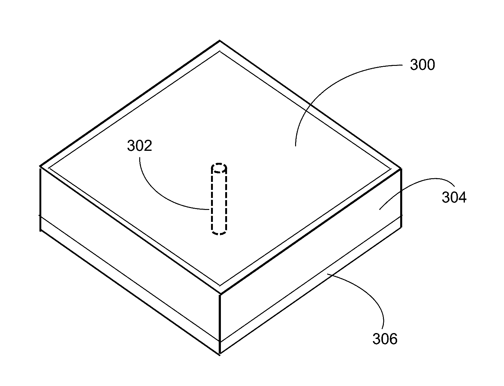
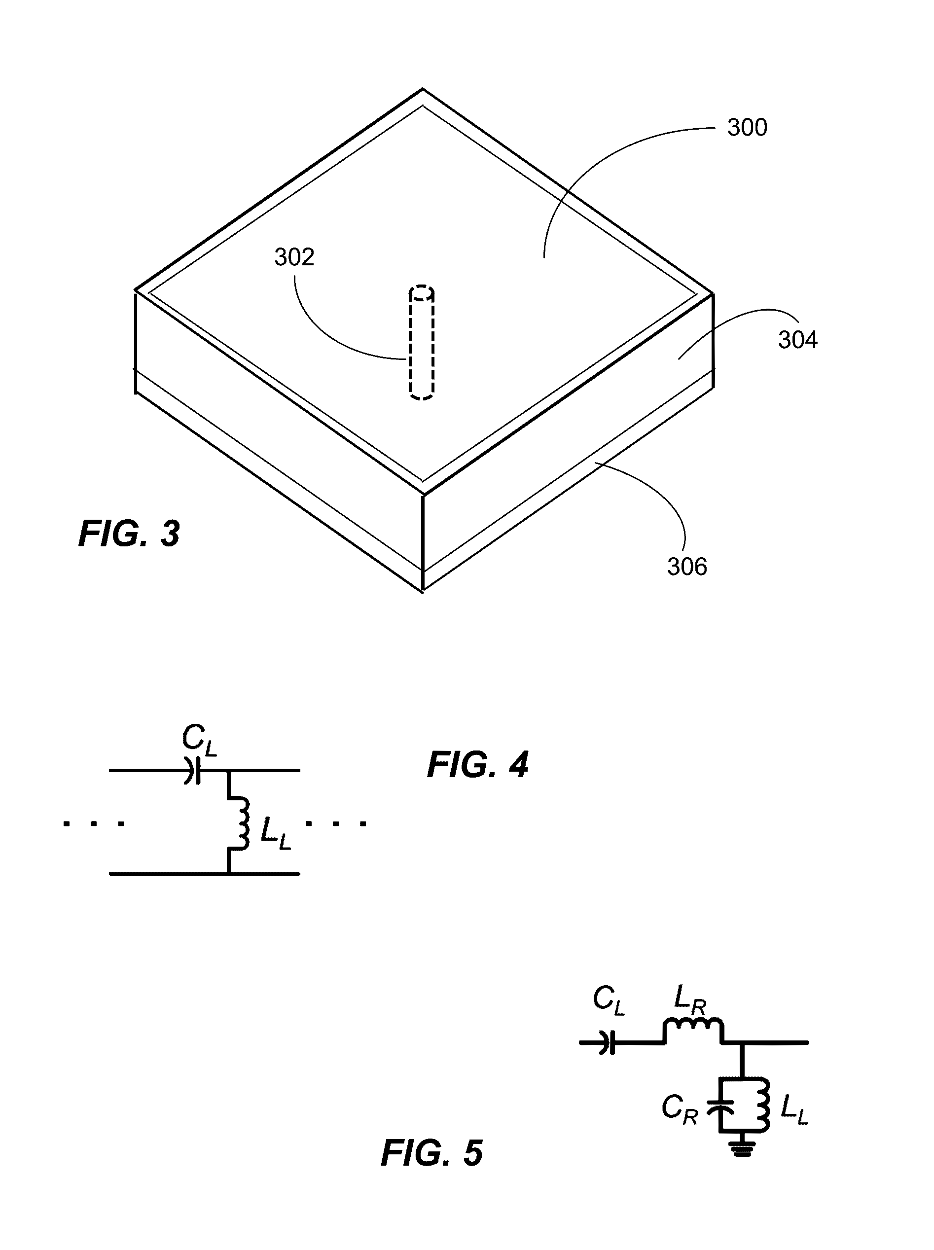
[0073]Metamaterial substrates are a new class of ordered artificial composites that exhibit ultra-thin dielectric thickness with exceptional electromagnetic properties not readily observed in conventional circuit materials that are used as ground, reference, or reflective planes in SiP modules and multilayer PCBs. Their precise shape, geometry, size, orientation, and arrangement can affect electromagnetic waves in a manner that exceeds the capabilities of conventional dielectric materials used in printed circuits. For example, their ultra-thin and ultra-small structure exhibit Electromagnetic Band Gaps (“EBG”) which can be integrated in microwave devices and SiP modules to improve performance. They can be used as circuit materials to design amplifiers, filters, power dividers, baluns, etc. They can be used in small outline and large format PCBs to provide reduced losses in transmission line structures. In addition to microwave devices, metamaterial substrates can be used in the desi...


PUM


Abstract

This invention enables Frequency Selective Surface (“FSS”) and Artificial Magnetic Conductor (“AMC”) which exhibits Electromagnetic Band Gap (“EBG”) in any of the substrate's layer from a small and thin systems and sub-systems in package to a large-format PCBs. The metamaterial substrate may be integrated with electronic circuit components or buried in PCBs for circuit designs capable of transmitting, receiving and reflecting electromagnetic energy, altering electromagnetic properties of natural circuit materials, enhancing electrical characteristics of electrical components (such as filters, antennas, baluns, power dividers, transmission lines, amplifiers, power regulators, and printed circuits elements) in systems and sub-systems circuit designs. The metamaterial substrate creates new electrical characteristics, properties and systems, sub-systems or component's specification not readily available with conventional circuit materials, substrates, and PCBs. The metamaterial substrate can be less than 70 μm thick and buried into any PCB layer.

Description

CROSS REFERENCE TO RELATED APPLICATIONS[0001]This application is a continuation of International Application Serial No. PCT / US2015 / 026733 filed Apr. 20, 2015, which claims the benefit of priority under 35 USC §119(e) to U.S. Provisional Patent Application No. 61 / 981,680 filed Apr. 18, 2014, the disclosures of which are incorporated herein by reference in their entireties.BACKGROUND OF THE INVENTION[0002]1. Field of the Invention[0003]This invention provides a metamaterial substrate which may be integrated with electronic circuit components and / or employed as a circuit layer in Printed Circuit Board and Wiring Board (collectively, “PCBs”) capable of transmitting, receiving and reflecting electromagnetic energy, altering electromagnetic properties of natural circuit materials, enhancing electrical characteristics of electronic components (such as filters, antennas, baluns, power dividers, transmission lines, amplifiers, power regulators, and printed circuit elements) in systems and su...

Claims


Application Information

Patent Timeline
IPC IPC(8): H01Q15/00H01Q19/00H01Q1/38
CPCH01Q15/0086H01Q19/005H01Q1/38H01P1/2005H01L2223/6677H01L2224/16227H01L2924/15321H01L2924/19105
Inventor WONG, CHIH WEI
Owner TRANSSIP
Learn More