
Semiconductor manufacturing apparatus and method for manufacturing semiconductor integrated circuit device
a manufacturing apparatus and semiconductor technology, applied in the direction of vacuum evaporation coating, chemical vapor deposition coating, epoxy resin and quartz ring, etc., can solve the problems of failure to meet the requirements dust emission, etc., and achieve the effect of improving the reliability of the semiconductor integrated circuit device and reducing the defect fraction
- Summary
- Abstract
- Description
- Claims
- Application Information
AI Technical Summary
Benefits of technology
Problems solved by technology
Method used
Image

Examples
first embodiment
[0030]First, a semiconductor manufacturing apparatus in this embodiment is explained taking a dry etching apparatus as an example, using FIG. 8 and FIG. 9. FIG. 8 is a plan view showing an overview of a dry etching apparatus DE. Moreover, FIG. 9 is a sectional view showing an outline of an etching chamber EC in FIG. 8.
[0031]Referring to FIG. 8, the dry etching apparatus of this embodiment is configured with a loader / unloader LU for carrying a wafer into / out of the apparatus, an atmosphere transfer chamber AT in which the wafer is transferred in air, a vacuum transfer chamber VT in which the wafer is transferred in vacuum, three etching chambers that are treatment chambers of the wafer, and one ashing chamber AC.
[0032]The wafers that were set in the loader / unloader LU are carried into the vacuum transfer chamber VT one sheet by one sheet by a robot arm RA of the atmosphere transfer chamber AT. The wafer carried into the vacuum transfer chamber VT is carried into any one of three etch...
second embodiment
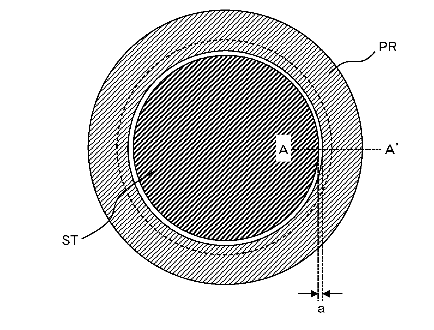
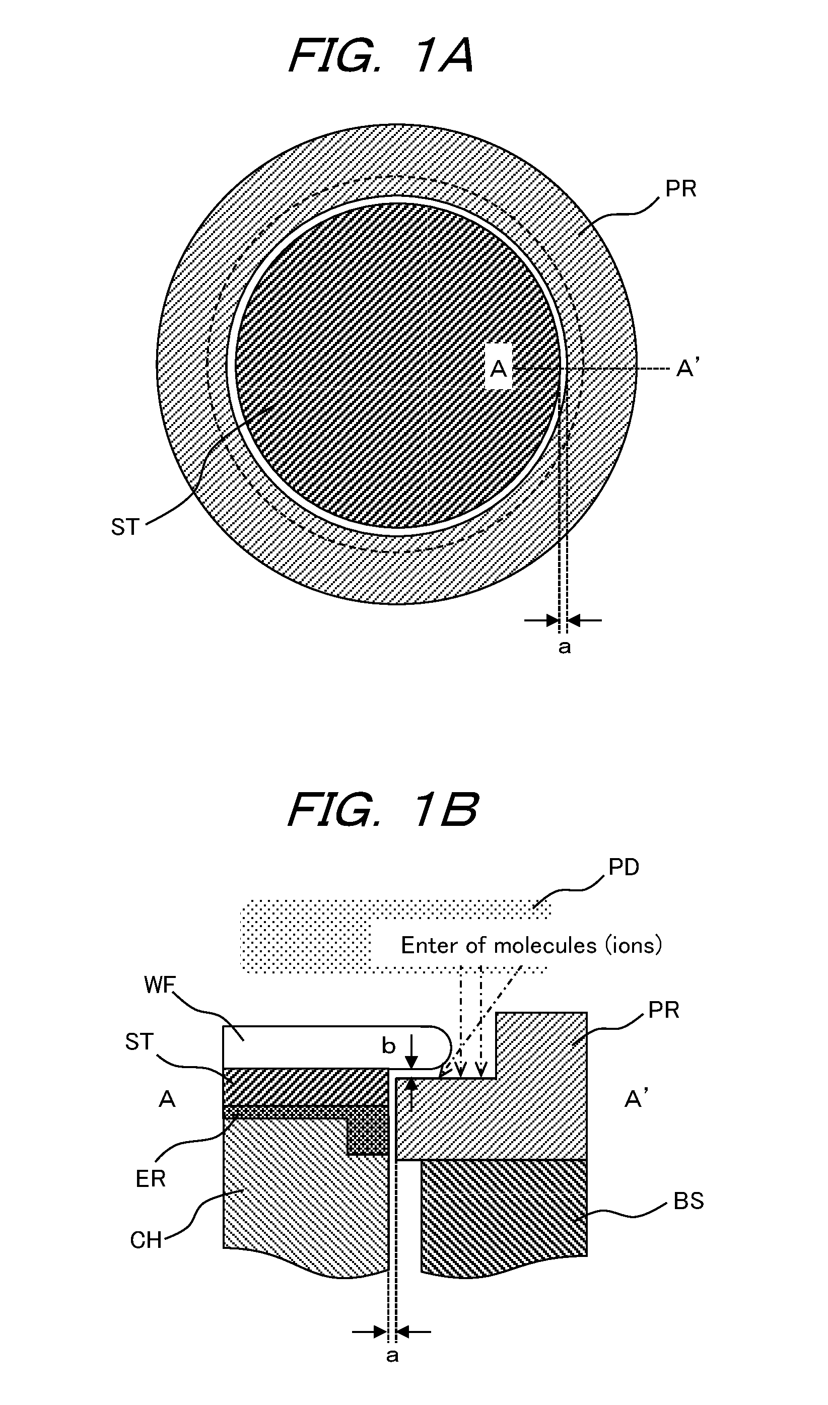
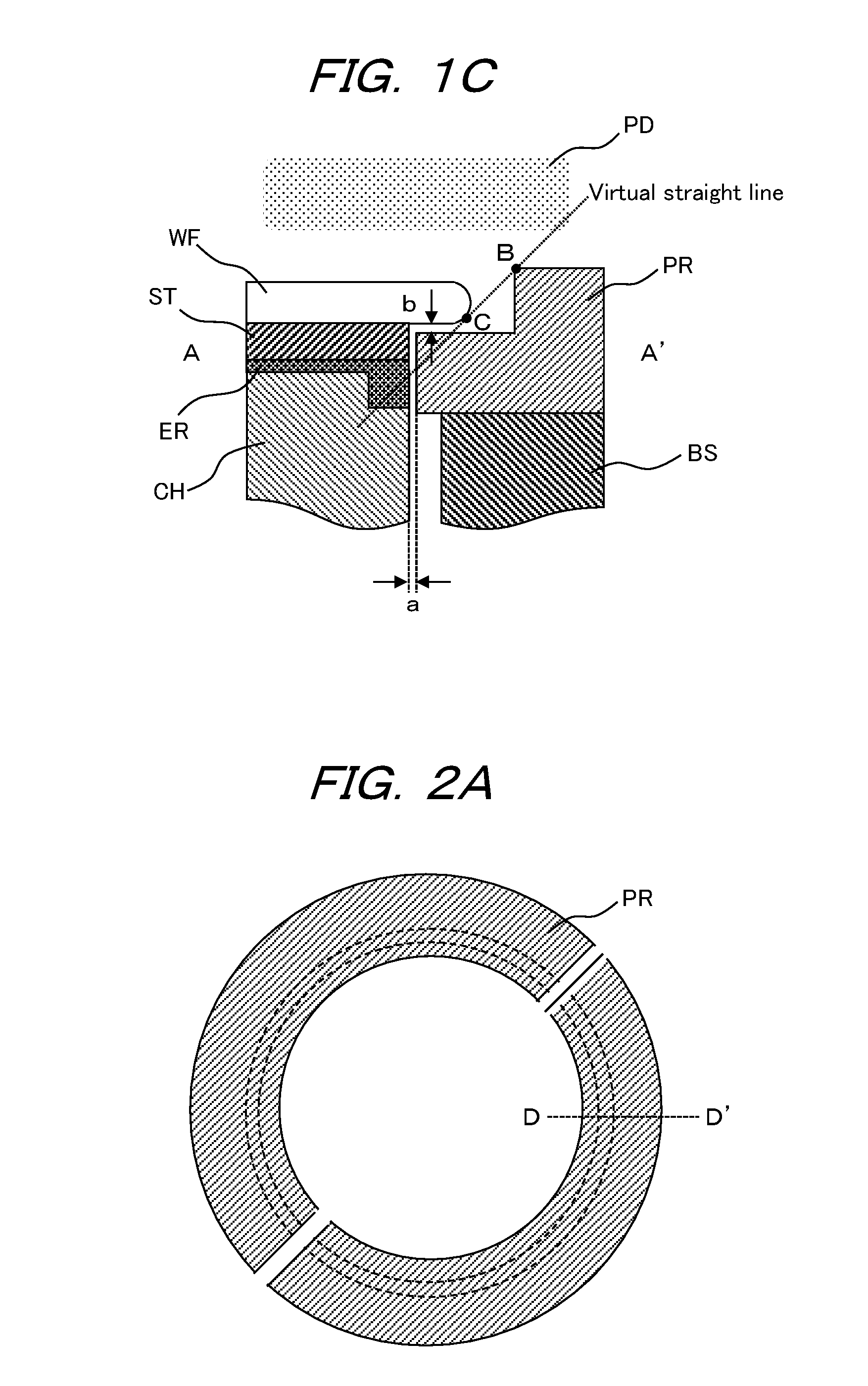
[0060]Configurations of the suction head CH and the circumference of the protection ring PR of this embodiment are explained using FIG. 2A to FIG. 4. FIG. 2B is an enlarged view of a section along a line D-D′ in FIG. 2A. However, in order to show a shape of the protection ring PR intelligibly, the wafer WF and the suction head CH (stage ST) are omitted in FIG. 2A. Moreover, FIG. 2C, FIG. 3, and FIG. 4 are modifications of FIG. 2B, respectively.
[0061]Referring to FIG. 2B, in the suction head CH of this embodiment, the ceramic plate, i.e., the stage ST, bonded to a position higher than the epoxy resin ER is formed to be wider than the aluminum base material. Moreover, the protection ring PR is formed to have multiple level differences according to a shape of the side face of the suction head CH.
[0062]Moreover, as shown in FIG. 2B, the protection ring PR has a side face whose end is close to the suction head CH (hereinafter, a lower region), a side face whose end is more distant from t...
third embodiment
[0071]A method for manufacturing a semiconductor integrated circuit device in this embodiment is explained using FIG. 5 to FIG. 7. FIG. 5 shows a dry etching process of processing a gate electrode GE of a transistor. Moreover, FIG. 6 shows a dry etching process of processing a contact hole CH for conducting the lower layer wiring and the upper wiring in the silicon oxide (SiO2) film that is an interlayer insulation film. FIG. 7 shows a dry etching process of processing aluminum wiring AW.
[0072]A dry etching process of a polysilicon film is explained with reference to FIG. 5. As shown in a left small figure of FIG. 5, a polysilicon film PS that becomes a target of dry etching is formed with a polysilicon film PS that is a film to be processed, an antireflection film (BARC) BC, and a photoresist pattern PP serving as an etching mask (mask pattern) at the time of the dry etching laminated sequentially from a lower layer on a silicon substrate SS.
[0073]The above-mentioned lamination str...
PUM
| Property | Measurement | Unit |
|---|---|---|
| Fraction | aaaaa | aaaaa |
| Distance | aaaaa | aaaaa |
| Mean free path | aaaaa | aaaaa |
Abstract
Description
Claims
Application Information