Semiconductor device, electronic component, and electronic device

a technology of semiconductor devices and electronic components, applied in pulse generators, pulse techniques, instruments, etc., can solve the problems of difficult to ensure a long data retention time, easy leakage of accumulated charge, and increase of leakage current flowing between a gate and a semiconductor layer, so as to achieve faster operation, lower power consumption, and high integration of a semiconductor device

Active Publication Date: 2017-02-23
SEMICON ENERGY LAB CO LTD
View PDF6 Cites 0 Cited by
  • Summary
  • Abstract
  • Description
  • Claims
  • Application Information

AI Technical Summary

Benefits of technology

[0009]To achieve lower power consumption, faster operation, or higher integration of a semiconductor device, a semiconductor element such as a transistor used in the semiconductor device needs to be reduced in size. As the size of transistors is reduced, the thickness of a gate insulating film is also reduced according to the scaling law. With a thinner gate insulating film, tunneling current occurs and thus leakage current flowing between a gate and a semiconductor layer increases.

Problems solved by technology

With a thinner gate insulating film, tunneling current occurs and thus leakage current flowing between a gate and a semiconductor layer increases.
In such a semiconductor device, when leakage current of the Si transistor increases because of reduction in transistor size, accumulated charge is easily leaked and it becomes difficult to ensure a long data retention time.

Method used


Image

  • Semiconductor device, electronic component, and electronic device
  • Semiconductor device, electronic component, and electronic device
  • Semiconductor device, electronic component, and electronic device

Examples


embodiment 1

[0048]This embodiment will explain an example of a semiconductor device that has a function of a nonvolatile memory device applicable to a register or the like.

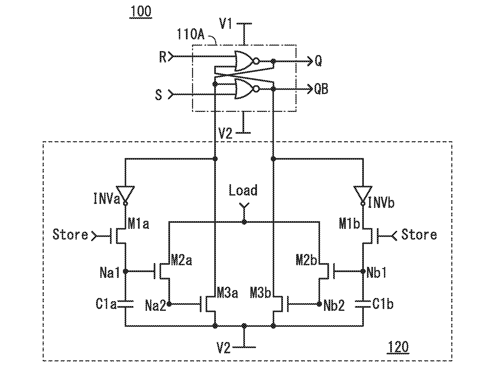
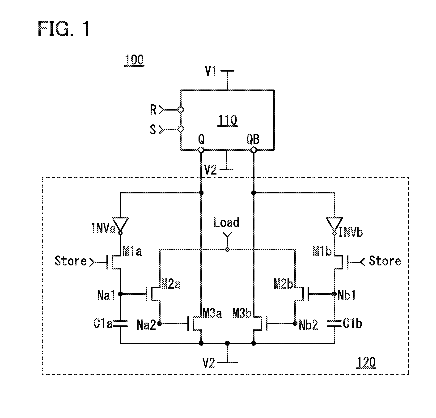
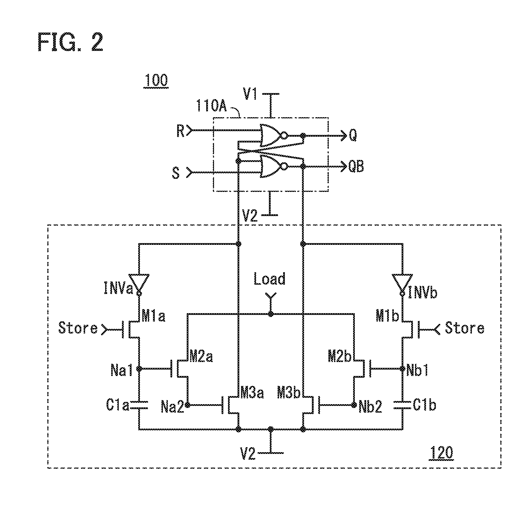
[0049]FIG. 1 is a circuit diagram illustrating an example of a circuit configuration of a semiconductor device 100. The semiconductor device 100 includes a circuit 110 and a circuit 120.

[0050]The circuit 110 has a function of storing data while power supply voltage is supplied. The circuit 120 has a function of storing data even while power supply voltage is not supplied.

[0051]The circuit 110 is a latch, for example. In FIG. 1, the circuit 110 is an SR latch having an input terminal R, an input terminal S, an output terminal Q, and an output terminal QB.

[0052]The circuit 120 is composed of a combination of a transistor containing an oxide semiconductor in its channel formation region (OS transistor) and a transistor containing silicon in its channel formation region (Si transistor), and stores data by holding charge correspon...

embodiment 2

[0085]This embodiment will explain the OS transistor described in the foregoing embodiment.

[0086]The off-state current of an OS transistor can be reduced by reducing the concentration of impurities in an oxide semiconductor to make the oxide semiconductor intrinsic or substantially intrinsic. The term “substantially intrinsic” refers to a state where an oxide semiconductor has a carrier density lower than 8×10¹¹ / cm3, preferably lower than 1×10¹¹ / cm3, more preferably lower than 1×10¹⁰ / cm3, and is higher than or equal to 1×10⁻⁹ / cm3. In the oxide semiconductor, hydrogen, nitrogen, carbon, silicon, and a metal element other than main components of the oxide semiconductor are impurities. For example, hydrogen and nitrogen form donor levels to increase the carrier density.

[0087]A transistor using an intrinsic or substantially intrinsic oxide semiconductor has a low carrier density and thus is less likely to have negative threshold voltage. In addition, because of few carrier traps in such...

embodiment 3

[0148]In this embodiment, a cross-sectional structure of a transistor included in a semiconductor device of one embodiment of the disclosed invention will be described with reference to drawings.

[0149]First, schematic views of a cross-sectional structure of the semiconductor device of one embodiment of the present invention will be described with reference to FIGS. 11A and 11B.

[0150]Transistors included in the semiconductor device of one embodiment of the present invention are Si transistors and OS transistors. For example, the semiconductor device has a cross-sectional structure in which a layer including Si transistors and a layer including OS transistors are stacked. Each of the layers includes a plurality of transistors including a semiconductor layer of the same material.

[0151]For example as illustrated in FIG. 11A, the semiconductor device of one embodiment of the present invention can be formed by stacking a layer 31 including Si transistors (represented as Si-FET Layer in FI...


PUM


Abstract

A semiconductor device that has a long data retention time during stop of supply of power supply voltage by reducing leakage current due to miniaturization of a semiconductor element. In a structure where charge corresponding to data is held with the use of low off-state current of a transistor containing an oxide semiconductor in its channel formation region, a transistor for reading data and a transistor for storing charge are separately provided, thereby decreasing leakage current flowing through a gate insulating film.

Description

BACKGROUND OF THE INVENTION[0001]1. Field of the Invention[0002]One embodiment of the present invention relates to a semiconductor device.[0003]Note that one embodiment of the present invention is not limited to the above technical field. The technical field of one embodiment of the invention disclosed in this specification and the like relates to an object, a method, or a manufacturing method. In addition, one embodiment of the present invention relates to a process, a machine, manufacture, or a composition of matter. Specific examples of the technical field of one embodiment of the present invention disclosed in this specification include a semiconductor device, a display device, a liquid crystal display device, a light-emitting device, a lighting device, a power storage device, a memory device, an imaging device, a method for driving any of them, and a method for manufacturing any of them.[0004]Note that in this specification, a semiconductor device refers to a device including a...

Claims


Application Information

Patent Timeline
Patent Type & Authority Applications(United States)
IPC IPC(8): G11C14/00H03K19/177H01L27/06H01L27/12
CPCG11C14/0054H01L27/1225H03K19/1776H01L27/0688H03K19/17764G11C11/24G11C14/00H03K3/356008Y02D10/00
Inventor AOKI, TAKESHIKOZUMA, MUNEHIROKUROKAWA, YOSHIYUKI
Owner SEMICON ENERGY LAB CO LTD
Why Eureka
Try Eureka