
Electronic device

a technology of electronic devices and insulating surfaces, applied in solid-state devices, synthetic resin layered products, light sources, etc., can solve the problems of insufficient gas barrier properties, achieve superior gas barrier properties and water vapor barrier properties, and resist physical stresses. high, the effect of high resistan

Inactive Publication Date: 2017-04-06
KURARAY CO LTD
View PDF4 Cites 24 Cited by
  • Summary
  • Abstract
  • Description
  • Claims
  • Application Information

AI Technical Summary

Benefits of technology

The present invention provides an electronic device with a protective sheet that resists physical stress, has excellent gas barrier properties, and prevents water vapor from entering or escaping. This protective sheet is also less likely to degrade over time in air, leading to a longer lifespan for the electronic device. Additionally, the invention includes a fluorescent quantum dot-containing electronic device that uses the protective sheet, which maintains its performance even after long-term use in air.

Problems solved by technology

However, the above conventional gas barrier layer may suffer from defects such as cracks and pinholes when exposed to physical stresses such as deformation and impact, and may thus fail to maintain sufficient gas barrier properties over a long period of time.
Even when fluorescent quantum dots are dispersed in a resin, however, they may be degraded, for example, by oxygen or water contained in air.

Method used


Image

  • Electronic device
  • Electronic device
  • Electronic device

Examples


first embodiment

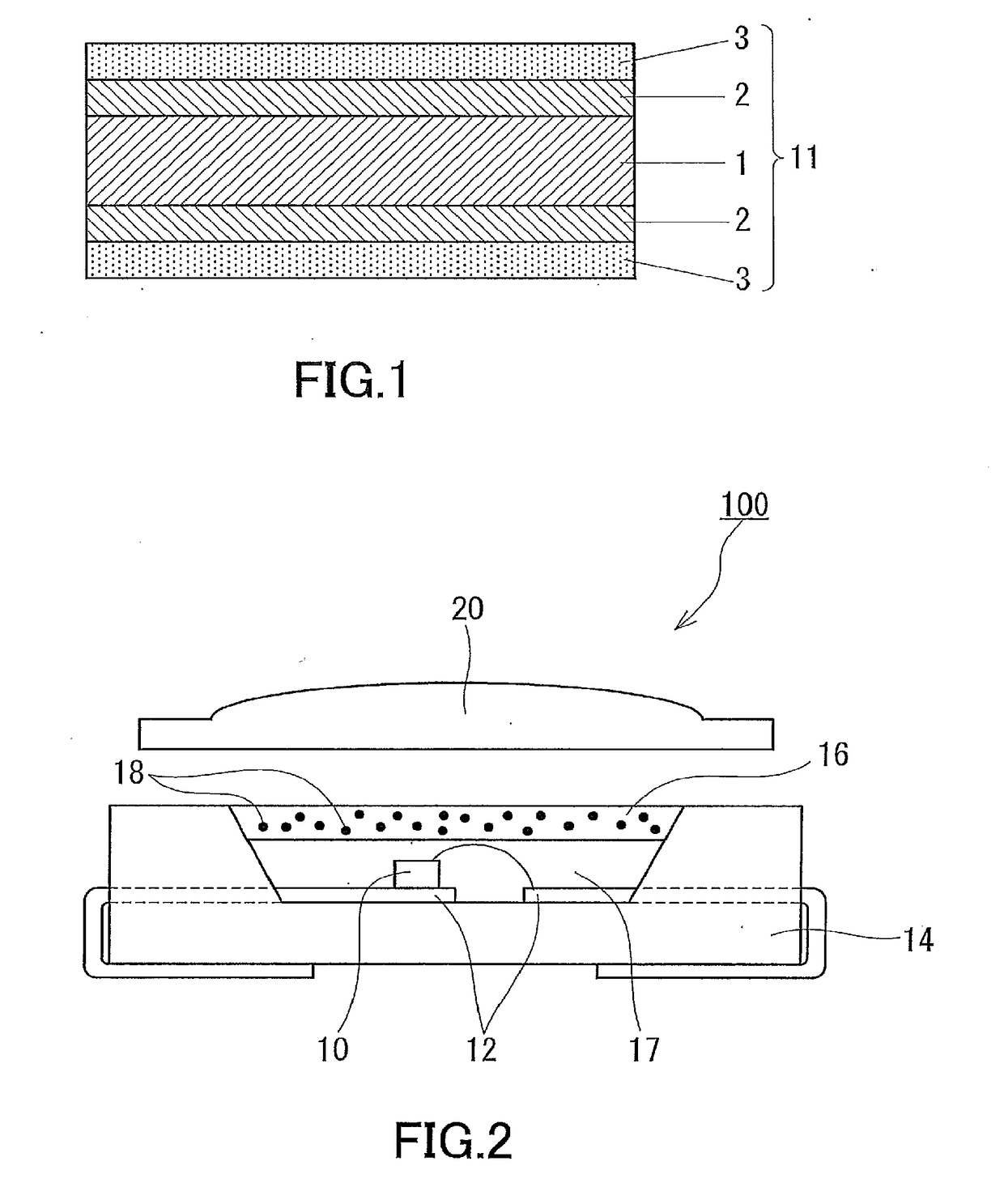
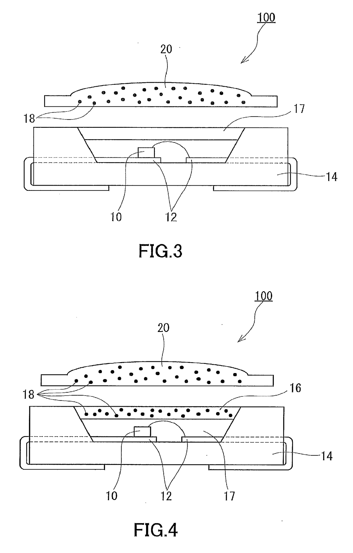
[0059]A fluorescent quantum dot-containing electronic device according to the first embodiment of the present invention employs a fluorescent quantum dot-dispersed resin shaped product. The fluorescent quantum dot-dispersed resin shaped product can be obtained by dispersing fluorescent quantum dots in a resin to prepare a dispersion (composition) and forming a shaped product from the dispersion. The method for shaping is not particularly limited, and a commonly-known method can be used. The resin as a dispersion medium is preferably a cycloolefin (co)polymer. Examples of the cycloolefin (co)polymer include a cycloolefin polymer (COP) represented by the formula [Q-1] given below and a cycloolefin copolymer (COC) represented by the formula [Q-2] given below. As such a cycloolefin (co)polymer there can be used as a commercially-available product. Examples of commercially-available products of the COP type include ZEONEX (registered trademark) series (manufactured by Zeon Corporation), ...

second embodiment

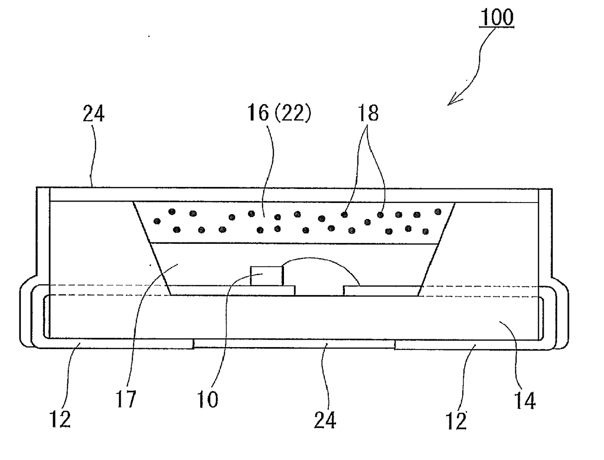
[0083]FIG. 5 shows a cross-sectional view of an example of a fluorescent quantum dot-containing structure according to the second embodiment. In FIG. 5, the fluorescent quantum dot-containing structure includes: a fluorescent quantum dot-dispersed resin shaped product 22 containing a resin as a dispersion medium and fluorescent quantum dots 18 dispersed in the resin at a concentration of 0.01 to 20 mass %; and a gas barrier layer (protective sheet) 24 covering the entire surface of the fluorescent quantum dot-dispersed resin shaped product 22 to reduce transmission of gas such as oxygen into the fluorescent quantum dot-dispersed resin shaped product 22. In another embodiment, the gas barrier layer 24 may be designed to cover a part of the surface of the fluorescent quantum dot-dispersed resin shaped product 22 (see FIGS. 6 and 7). It is preferable for the gas barrier layer 24 to be capable of reducing transmission of not only oxygen but also water vapor.

[0084]The gas barrier layer 2...

example 1

[Example 1]

[0348]First, a PET 12 was prepared as the base (X). The first coating liquid (U-1) was applied onto this base using a bar coater in such a manner that the dry thickness would be 0.5 μm, and the applied film was dried at 100° C. for 5 minutes to form a precursor layer of the layer (Y) on the base. This was followed by heat treatment at 180° C. for 1 minute to form the layer (Y). In this way, a multilayer structure (1-1) having a configuration of “layer (Y) (0.5 μm) / PET” was obtained.

[0349]As a result of measurement of the infrared absorption spectrum of the multilayer structure (1-1), the maximum absorption wavenumber in the region of 800 to 1,400 cm−1 was determined to be 1,107 cm−1, and the half width of the maximum absorption band in the same region was determined to be 37 cm−1. The result is shown in Table 1.

[0350]As a result of quantitative analysis of sodium ions contained in the multilayer structure (1-1), the value of {(ionic charge of sodium ions)×(num...


PUM

PropertyMeasurementUnit
Temperatureaaaaaaaaaa
Fluorescenceaaaaaaaaaa
Thermoplasticityaaaaaaaaaa

Abstract

The present invention relates to an electronic device having an electronic device body 1 the surface of which is covered by a protective sheet. The protective sheet includes a multilayer structure including a base (X) and a layer (Y) stacked on the base (X). The layer (Y) includes a metal oxide (A), a phosphorus compound (B), and cations (Z) with an ionic charge (FZ) of 1 or more and 3 or less. The phosphorus compound (B) includes a compound containing a moiety capable of reacting with the metal oxide (A). In the layer (Y), the number of moles (NM) of metal atoms (M) constituting the metal oxide (A) and the number of moles (NP) of phosphorus atoms derived from the phosphorus compound (B) satisfy a relationship of 0.8≦NM / NP≦4.5, and NM, the number of moles (NZ) of the cations (Z), and FZ satisfy a relationship of 0.001≦FZ×NZ / NM≦0.60.

Description

TECHNICAL FIELD[0001]The present invention relates to electronic devices. The present invention more particularly relates to an electronic device including a protective sheet including a multilayer structure including a base (X) and a layer (Y) stacked on the base (X). The present invention also relates to a fluorescent quantum dot-containing electronic device including a protective sheet including a multilayer structure including a base (X) and a layer (Y) stacked on the base (X).BACKGROUND ART[0002]Composite structures having a gas barrier layer containing aluminum have conventionally been proposed for use in electronic devices such as a liquid crystal display of a display device, and examples of the composite structures include a composite structure having a transparent gas barrier layer composed of a product of reaction between aluminum oxide particles and a phosphorus compound (see Patent Literature 1).[0003]Patent Literature 1 discloses a method for forming the gas barrier lay...

Claims


Application Information

Patent Timeline
IPC IPC(8): C08J7/04H01L33/56C09D129/04H01L33/62C09D7/12H01L33/54H01L33/50C08J7/043C08J7/046C08J7/048C08J7/052C09D7/61
CPCC08J7/047H01L33/54H01L33/56H01L33/507H01L33/62C08J2443/02C09D129/04C08J7/042C08J2367/02C08J2429/04C08J2433/14C09D7/1216C09D1/00H01L2224/48091H01L2224/48247H01L2924/181C09K11/025C09K11/703H05B33/04H05B33/20B32B7/12B32B23/08B32B27/08B32B27/28B32B27/281B32B27/285B32B27/286B32B27/288B32B27/302B32B27/306B32B27/308B32B27/32B32B27/34B32B27/36B32B27/365B32B2250/04B32B2255/10B32B2255/20B32B2307/31B32B2307/412B32B2307/418B32B2307/422B32B2307/518B32B2307/7244B32B2307/7246B32B2307/73B32B2457/00B32B2457/202C09D7/40C09D7/61C08J7/048C08J7/052C08J7/043C08J7/046C08J7/0427H01L2924/00014H01L2924/00012H01L33/06H01L33/502H01L33/58H01L2933/005H01L2924/12041B32B27/00
Inventor SASAKI, RYOICHIINUBUSHI, YASUTAKANAKAYA, MASAKAZUTAKAI, JUNARIMOTO, KIKUOOTA, MASAHIKOMORIHARA, YASUSHI
Owner KURARAY CO LTD
Learn More