Semiconductor device and electronic device

a technology of semiconductor devices and electronic devices, applied in the field of semiconductor devices, can solve the problems of increasing the chip area, difficult to configure ideal analog memory, and extremely short data holding, and achieve the effects of small chip area, novel structure, and reduced power consumption

Inactive Publication Date: 2017-04-27
SEMICON ENERGY LAB CO LTD
View PDF19 Cites 23 Cited by
  • Summary
  • Abstract
  • Description
  • Claims
  • Application Information

AI Technical Summary

Benefits of technology

[0017]Alternatively, an object of one embodiment of the present invention is to provide a semiconductor device or the like with a novel structure and a small chip area. Alternatively, an object of one embodiment of the present invention is to provide a semiconductor device or the like with a novel structure, in which power consumption is reduced.
[0024]One embodiment of the present invention can provide a novel semiconductor device, a novel display device, a novel electronic device, or the like.
[0025]Alternatively, one embodiment of the present invention can provide a semiconductor device or the like with a novel structure and a small chip area. Alternatively, one embodiment of the present invention can provide a semiconductor device or the like with a novel structure and lower power consumption.

Problems solved by technology

Meanwhile, in the case where the memory, the multiplier circuit, and the adder circuit are formed using analog circuits, although the number of circuit elements can be reduced, it is extremely difficult to configure an ideal analog memory, that is, an analog memory capable of holding an analog value, as the memory.
In the case of using a dynamic random access memory (DRAM) type analog memory, data holding is extremely short.
However, these configurations cause an increase in a chip area and an increase in power consumption.

Method used


Image

  • Semiconductor device and electronic device
  • Semiconductor device and electronic device
  • Semiconductor device and electronic device

Examples


embodiment 1

[0066]Embodiments of the present invention are described with reference to FIG. 1, FIGS. 2A to 2D, FIG. 3, FIGS. 4A to 4E, FIG. 5, FIGS. 6A to 6E, FIGS. 7A to 7D, FIGS. 8A to 8D, FIG. 9. FIG. 10, FIG. 11, and FIGS. 12A and 12B.

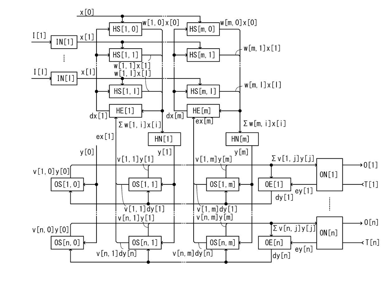
[0067]FIG. 1 is a block diagram of a semiconductor device. FIG. 1 shows the semiconductor device including / input neuron circuits IN (l is a natural number), m hidden neuron circuits HN (m is a natural number), n output neuron circuits ON (n is a natural number), (l+1)×m hidden synapse circuits HS, (m+1)×n output synapse circuits OS, m hidden error circuits HE, and n output error circuits OE.

[0068]The block diagram in FIG. 1 is described below.

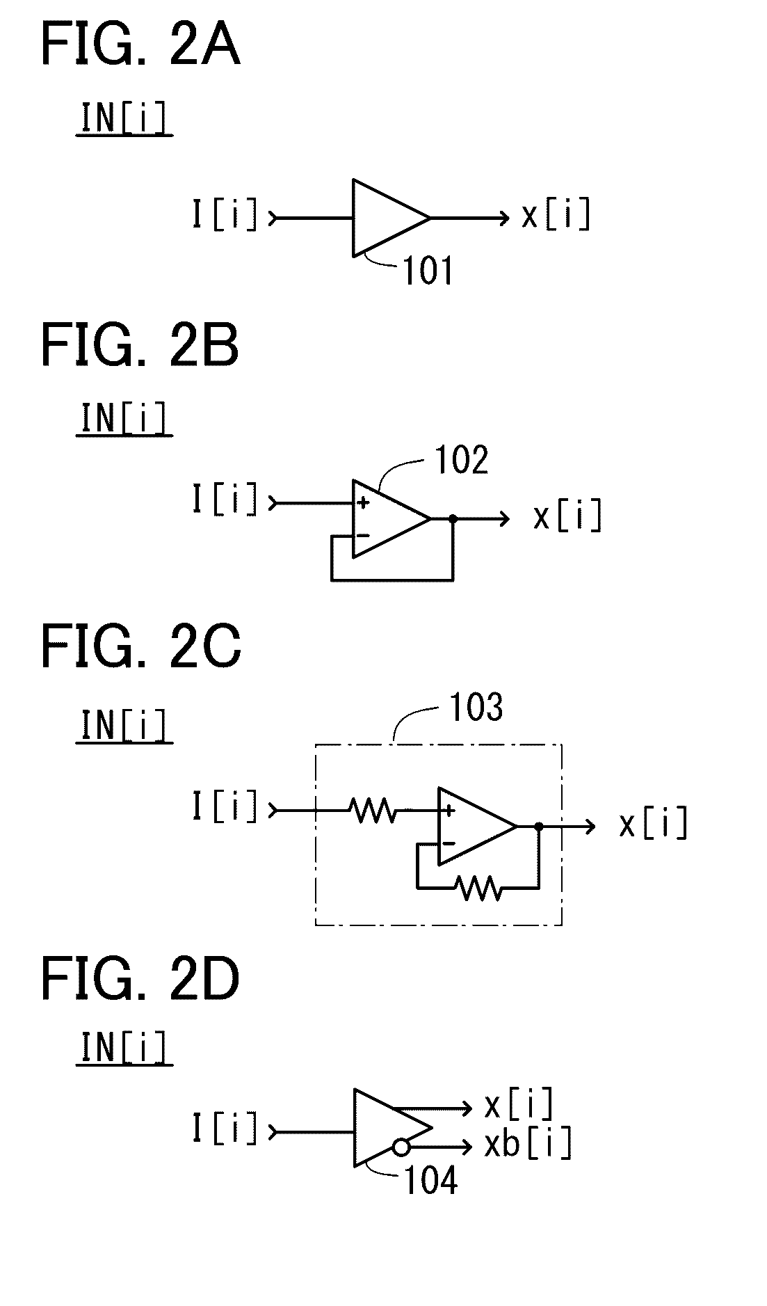
[0069]FIG. 2A shows a configuration of an input neuron circuit IN[i]. The input neuron circuit IN[i] includes an amplifier 101 which amplifies an input signal I[i] from the outside of the semiconductor device to generate an output signal x[i]. Note that as shown in FIG. 2B, a unity gain buffer 102 may be used instead of t...

embodiment 2

[0103]In this embodiment, an operation example of the semiconductor device in FIG. 1 is described.

[0104]The operation of the semiconductor device refers to operation in which learning data is input to the semiconductor device described in Embodiment 1 in FIG. 1 so that the semiconductor device learns the learning data, object data is input to the semiconductor device, and judgment whether the learning data and the object data match, are similar, or mismatch is made. FIG. 13 and FIG. 14 are flowcharts of the operation of the semiconductor device. The operation of the semiconductor device in FIG. 1 is described as an example below.

>

[0105]First, operation where the semiconductor device learns data is described with reference to FIG. 1 and FIG. 13.

[Step S1-1]

[0106]In Step S1-1, learning data is input from the outside to the neuron circuit IN. Note that learning data correspond to input signals I[1] to I[l] in FIG. 1. Note that leaning data is represented in binary here, and the number o...

embodiment 3

[0159]In this embodiment, a broadcast system according to the disclosed invention will be described.

[0160]FIG. 17 is a block diagram schematically illustrating a configuration example of a broadcast system. A broadcast system 500 includes a camera 510, a transmitter 511, a receiver 512, and a display device 513. The camera 510 includes an image sensor 520 and an image processor 521. The transmitter 511 includes an encoder 522 and a modulator 523. The receiver 512 includes a demodulator 525 and a decoder 526. The display device 513 includes an image processor 527 and a display portion 528.

[0161]When the camera 510 is capable of taking an 8K video, the image sensor 520 includes a sufficient number of pixels to capture an 8K color image. For example, when one red (R) subpixel, two green (G) subpixels, and one blue (B) subpixel are included in one pixel, the image sensor 520 with an 8K camera needs at least 7680×4320×4 [R, G+G, and B] pixels, the image sensor 520 with a 4K camera needs ...


PUM


Abstract

A semiconductor device with a novel structure is provided. Input neuron circuits, hidden neuron circuits, and output neuron circuits are hierarchically connected to one another through plural synapse circuits. Each synapse circuit includes an analog memory which stores data corresponding to a connection strength between the input neuron circuit and the hidden neuron circuit or between the hidden neuron circuit and the output neuron circuit, a writing circuit which changes the data in the analog memory, and a weighting circuit which outputs an output signal obtained by weighting an input signal in accordance with data in the analog memory. The analog memory is formed using a transistor including an oxide semiconductor having extremely low off-state current. It is not necessary to mount a large-scale capacitor for holding data and to recover analog data by regular refresh operation; thus, reduction in a chip area and reduction in power consumption are possible.

Description

TECHNICAL FIELD[0001]One embodiment of the present invention relates to a semiconductor device or an electronic device which includes the semiconductor device.[0002]Note that one embodiment of the present invention is not limited to the above technical field. The technical field of the invention disclosed in this specification and the like relates to an object, a method, or a manufacturing method. Furthermore, one embodiment of the present invention relates to a process, a machine, manufacture, or a composition of matter. Specifically, examples of the technical field of one embodiment of the present invention disclosed in this specification include a semiconductor device, a display device, a light-emitting device, a power storage device, a memory device, a method for driving any of them, and a method for manufacturing any of them.[0003]In this specification and the like, a semiconductor device refers to an element, a circuit, a device, or the like that can function by utilizing semi...

Claims


Application Information

Patent Timeline
Patent Type & Authority Applications(United States)
IPC IPC(8): H04N19/423H01L29/24G06N3/04H04N19/543H04N19/43G11C27/00H01L29/786H04N19/527
CPCH04N19/423H01L29/7869H01L29/78696H01L29/78642H01L29/78648G06N3/04H04N19/527H04N19/543H04N19/43G11C27/005H01L29/24H01L27/1225G06T9/002G11C27/024H04N19/90G06N3/063G06N3/08
Inventor KUROKAWA, YOSHIYUKI
Owner SEMICON ENERGY LAB CO LTD
Why Eureka
Try Eureka