Compound for organic electronic element, organic electronic element comprising the same, and electronic device thereof
a technology of electronic elements and organic electric elements, which is applied in the direction of luminescent compositions, organic chemistry, chemistry apparatus and processes, etc., can solve the problems of power consumption, efficiency and life span issues, and the need for power consumption to increase, so as to improve the energy level and high t1 value of the hole, and improve the efficiency of organic electric elements. , the effect of high t1 value and high energy level
- Summary
- Abstract
- Description
- Claims
- Application Information
AI Technical Summary
Benefits of technology
Problems solved by technology
Method used
Image
Examples
synthesis example
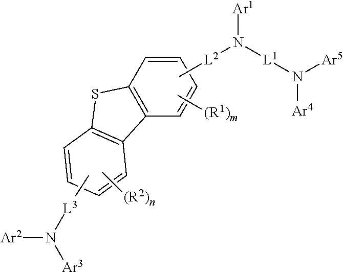
[0093]The compound (final products) represented by Formula 1 according to the present invention are synthesized by reacting Sub 1 and Sub 2 as shown in Reaction Scheme 1, but are not limited thereto.
[0094]Ar1 to Ar5, L1 to L3, R1, R2, m, n, and the like are the same as defined in Formula 1.
[0095]I. Synthesis of Sub 1
[0096]Sub 1 of the above Reaction Scheme 1 is synthesized by the following Reaction Scheme 2, but is not limited thereto. Hal1 is I, Br or Cl, and Hal2 is Br or Cl.
[0097]In the Reaction Scheme 2, the amine(HN—Ar2Ar3) reactant was synthesized by using the synthesis method disclosed in Korean Patent No. 10-1251451 (published on Apr. 5, 2013) of the present applicant.
[0098]Synthesis Examples of compounds belonging to Sub 1 are as follows.
1. Synthesis Examples of Sub 1-1 and Sub 1-83
[0099]
[0100](1) Synthesis of Sub 1-III-1
[0101]After the starting material diphenylamine (CAS Registry Number: 122-39-4) (17.24 g, 101.87 mmol) was dissolved in toluene (850 ml) in a round bottom ...
example 1
[Example 1] Green OLED (a Hole Transport Layer)
[0227]Organic light emitting diodes (OLEDs) were fabricated according to a conventional method by using a compound of the present invention as a hole transport layer material.
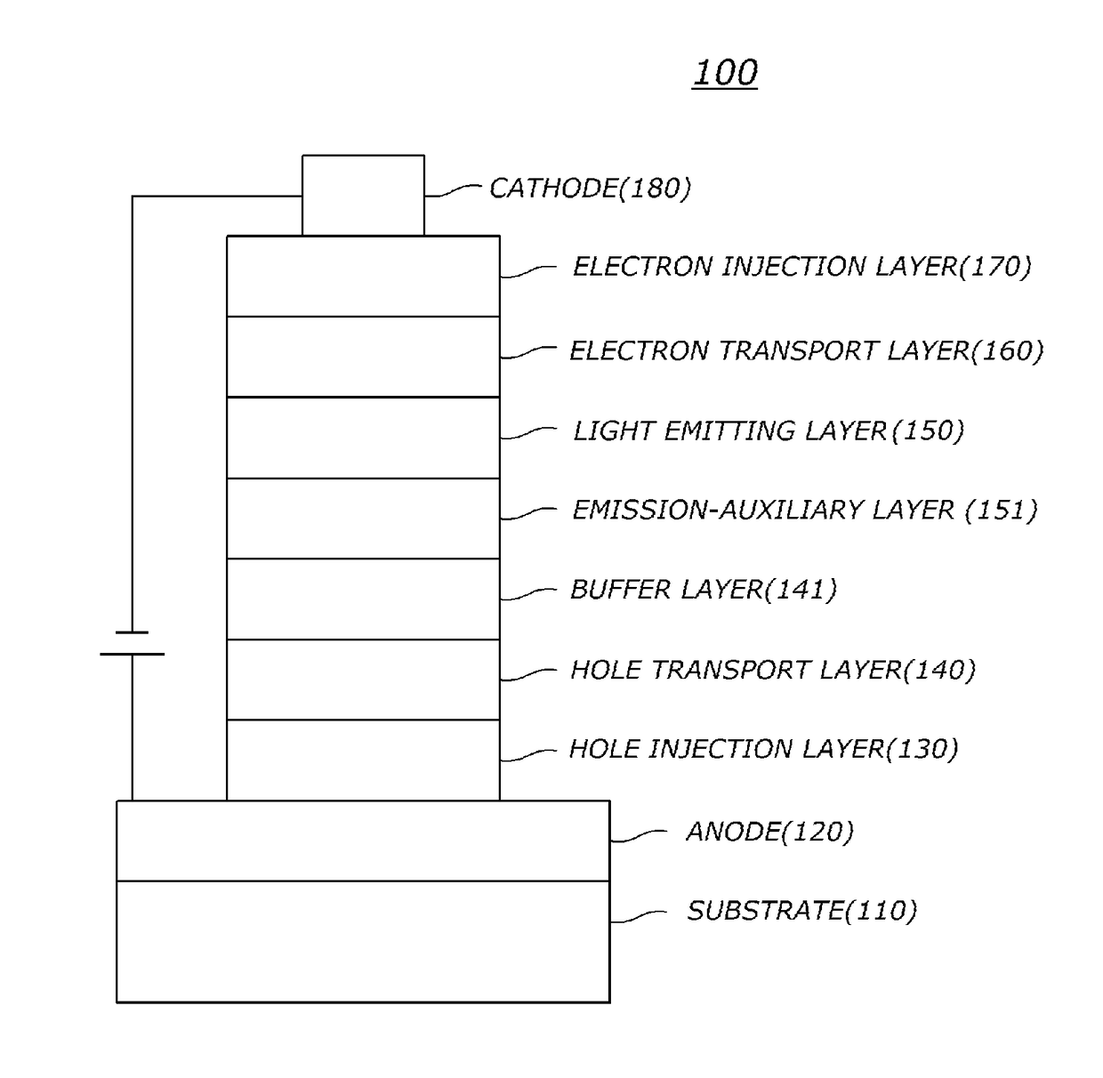
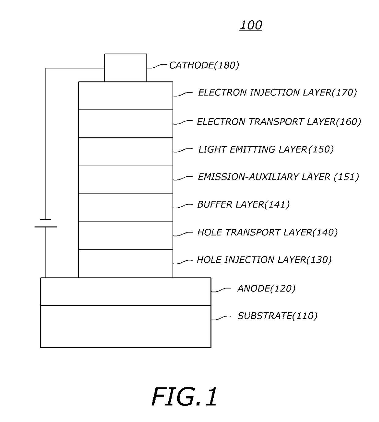
[0228]First, an ITO layer (anode) was formed on a glass substrate, and then 4,4′,4″-tris[2-naphthyl(phenyl)amino]triphenylamine (hereinafter, “2-TNATA”) was vacuum-deposited on the ITO layer to form a hole injection layer with a thickness of 60 nm.
[0229]Subsequently, compound P-1 of the present invention was vacuum-deposited with a thickness of 60 nm on the hole injection layer to form a hole transport layer.
[0230]Subsequently, a light emitting layer with a thickness of 30 nm was formed on the hole transport layer by using 4,4′-N,N′-dicarbazole-biphenyl (hereinafter, “CBP”) as a host material and tris(2-phenylpyridine)-iridium (hereinafter, “Ir(ppy)3)”) as a dopant material in a weight ratio of 90:10.
[0231]Next, ((1,1′-bisphenyl)-4-olato)bis(2-methyl-8-quinolinolat...
example 33
[Example 2] to [Example 33] Green OLED (a Hole Transport Layer)
[0233]The OLEDs were fabricated in the same manner as described in Example 1 except that the compounds P-6 to P-134 of the present invention described in Table 4 instead of the compound P-1 of the present invention were used as the hole transport layer material.
PUM
| Property | Measurement | Unit |
|---|---|---|
| thickness | aaaaa | aaaaa |
| thickness | aaaaa | aaaaa |
| thickness | aaaaa | aaaaa |
Abstract
Description
Claims
Application Information


