Method for manufacturing a resistive device for a memory or logic circuit

a resistive device and logic circuit technology, applied in solid-state devices, vacuum evaporation coatings, coatings, etc., can solve the problems of reproducibility and defectiveness, gas used to generate reactive plasma may corrode the materials to be etched, and ibe (ion beam etching) to achieve the effect of reducing electrical variability

Active Publication Date: 2017-10-26
COMMISSARIAT A LENERGIE ATOMIQUE ET AUX ENERGIES ALTERNATIVES +2
View PDF22 Cites 16 Cited by
  • Summary
  • Abstract
  • Description
  • Claims
  • Application Information

AI Technical Summary

Benefits of technology

[0016]There thus exists a need to provide a method for manufacturing a resistive device leading to lower variability in electrical and retention properties between storage elements.

Problems solved by technology

These residues also have a tendency to line the walls of the etching frame, leading to problems of reproducibility and defectiveness.
In addition, the gases used to generate the reactive plasma may corrode the materials to be etched.
Nevertheless, this technique, known as IBE (Ion Beam Etching), gives results of insufficient quality for an industrial method.
Indeed, several problems are posed:The IBE technique leads to a high number of defects at the edges of the structures that form the storage elements and to an important variability in electrical or magnetic properties from one memory point to another.Since the etching residues are not volatile, they pollute the substrate and the etching frame, like plasma etching.
In particular, they are deposited on the sides of the structures, which alter the electrical properties of the storage elements.
For example, in the case of a magnetic tunnel junction, etching of the upper magnetic electrode may lead to metal deposition on the sides of the structure, which short-circuit the tunnel barrier.Storage elements etched by IBE have inclined sides, which is a hindrance for high density applications where the memory points are very close to each other.Uniform etching on substrates of diameter greater than or equal to 300 mm is difficult to obtain, because the flux of ions is not homogeneous on such a surface.
No solution has thus been found until now for etching, in a satisfactory manner, the materials of storage elements used in MRAM, OxRAM and CBRAM non-volatile memories, notably those of resolution less than 30 nm.
Furthermore, the same problems are posed in the field of logic components, and more particularly MLU (Magnetic Logic Units) which each comprise a magnetic tunnel junction etched by IBE or reactive plasma etching.
Nevertheless, successive depositions of materials on the sides of the cavities reduce the effective surface of the storage element and makes the control of the thickness of the layers deposited on these sides difficult.
If the thickness of the barrier layer becomes too low at the level of the sides of the cavities, electrical short-circuits may occur through this barrier, making the tunnel junction unusable.
Despite the absence of etching, this structuring method generates in the memory points (or logic points) structural and / or chemical defects, which lead to a high variability in point to point properties, in particular a high dispersion of the electrical and retention properties of the memory point (that is to say its capacity to store information over time).

Method used


Image

  • Method for manufacturing a resistive device for a memory or logic circuit
  • Method for manufacturing a resistive device for a memory or logic circuit
  • Method for manufacturing a resistive device for a memory or logic circuit

Examples


first embodiment

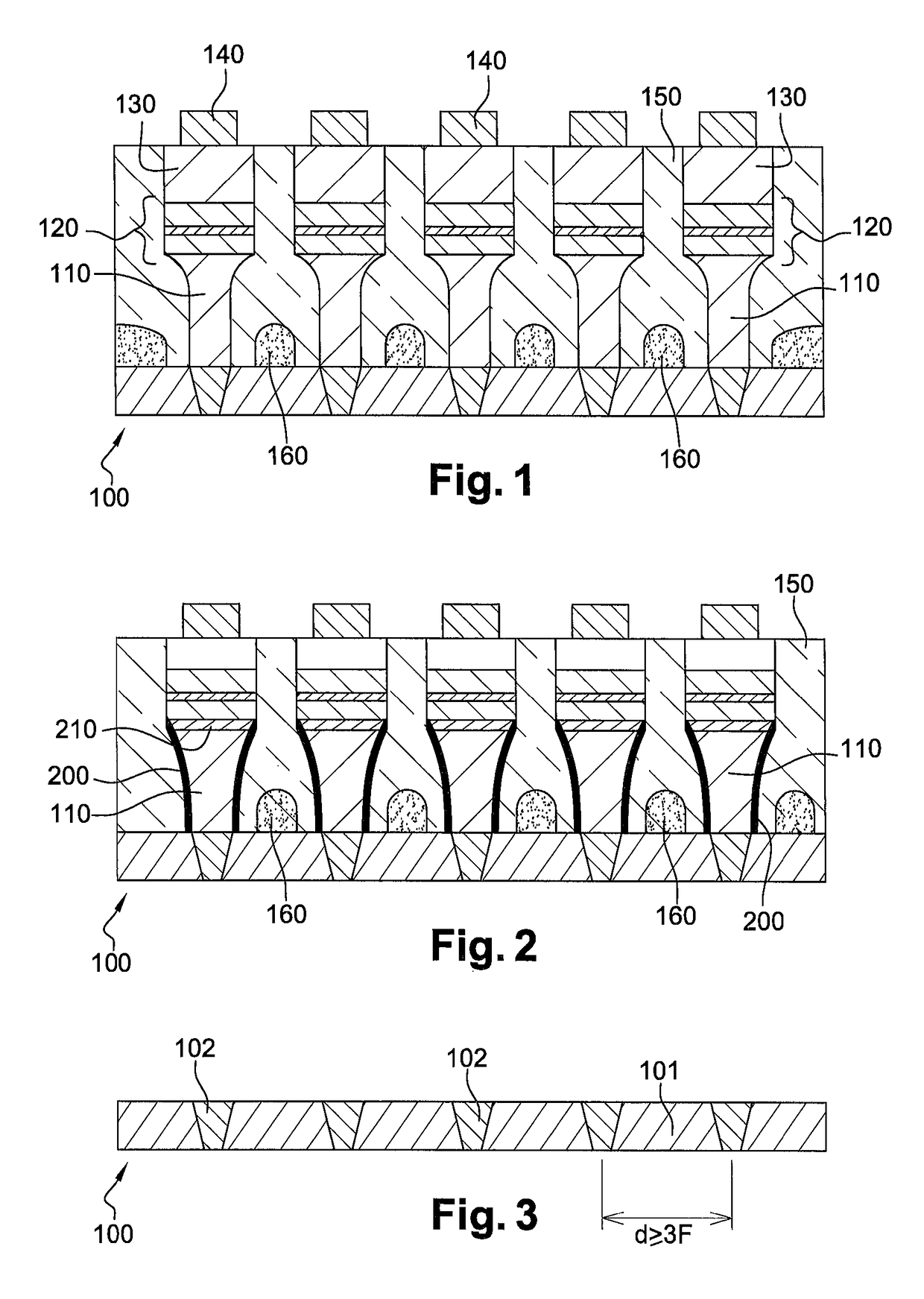
[0056]FIG. 1 represents, in section view, a resistive device where the variable resistance storage elements are supported by flared conductive pillars.

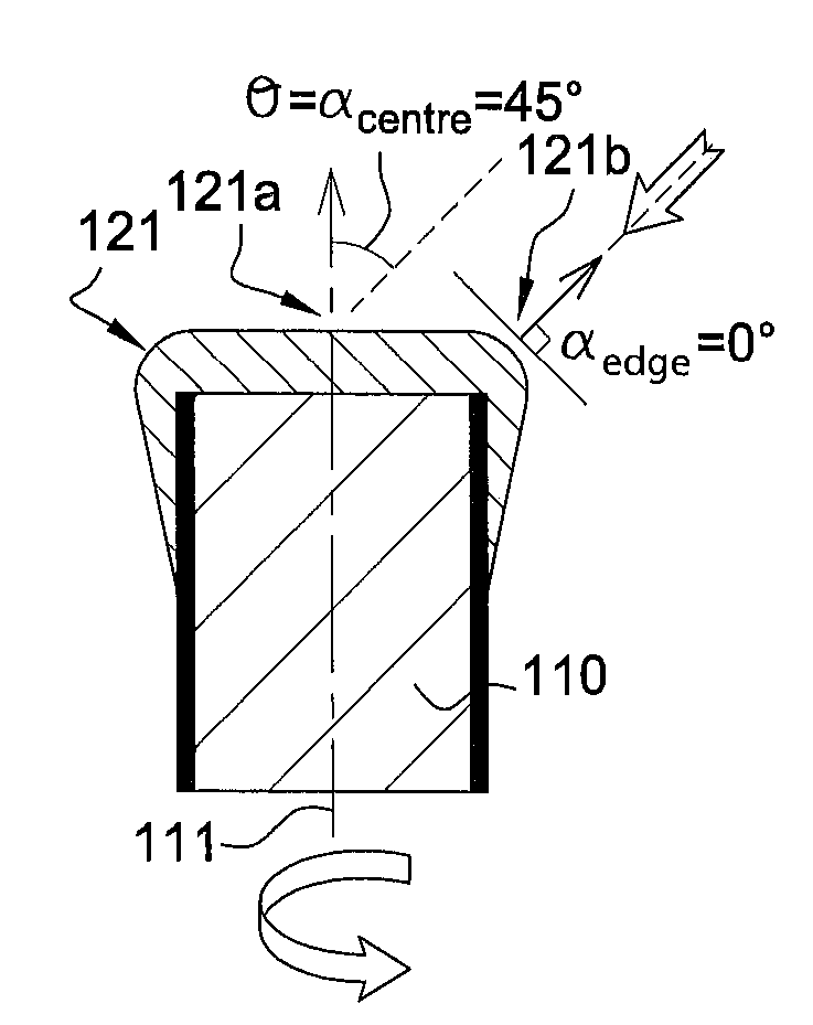
[0057]The resistive device comprises a substrate 100 on which is arranged a set of pillars 110 made of electrically conductive material, for example tantalum. The pillars 110 are oriented vertically with respect to the plane of the substrate 100. Preferably, their section, measured in a plane parallel to the substrate 100, varies in a strictly increasing manner from the base to the top of the pillars. In other words, the section of the pillars 110 is minimum at their base and maximum at their top.

[0058]The device further comprises a plurality of storage elements 120 arranged at the tops of the pillars 110. In the case of memory type applications, these storage elements 120 have an electrical resistance varying between two states in response to an electric stimulus, a low resistance state and a high resistance state. They may thus form...

second embodiment

[0064]FIG. 2 represents a second embodiment, wherein the sides of the pillars 110 have an arc of circle or “bowing” shape and are covered with a layer 200 made of electrically insulating material. The section of the pillars varies in a continuous manner, for example increasing from the base to the top of the pillars, as is illustrated in FIG. 2. Otherwise, the section may decrease slightly from the base of the pillars then increase on approaching the top. In other words, the minimum section of the pillars is not necessarily that at the base of the pillars.

[0065]More generally, the pillars may be of varied shapes depending on the technology used. In particular, their section may be round, elliptical, square or rectangular.

[0066]The insulating layer 200 covers at least the portion of side situated at the base of the pillars 110, facing the residual deposits 160 of resistive material, and preferably the totality of the sides. It improves the electrical insulation between the different ...

third embodiment

[0118]It may be noted in the sectional view of FIG. 5 that, when they are produced according to the “damascene” method, the electrical contacts 140 and the conductive vias 102 of the substrate 100 also have a flared shape, with a section at the base smaller than at their top. By their very shape, the conductive vias of damascene type could thus serve as support to the variable resistance storage elements. Thus, in the resistive device, the flared conductive pillars are constituted of electrical interconnection vias of damascene type.

[0119]In FIG. 6, the pillars are advantageously formed by the upper part of conductive vias 102′ belonging to the final interconnection level of the substrate 100 (before the memory points). In other words, the conductive vias 102′ are extended outside of the dielectric layer 101 and serve as support to the deposition of the storage elements 120 and the covering elements 130, before being surrounded by the dielectric filling material 150.

[0120]Alternativ...


PUM

PropertyMeasurementUnit
polarisation voltageaaaaaaaaaa
diameteraaaaaaaaaa

Abstract

A method for manufacturing a resistive device, includes depositing a first electrically conductive layer on a substrate; forming an etching mask on the first conductive layer; etching the first conductive layer through the mask, such as to obtain a plurality of electrically conductive pillars separated from one another; and forming storage elements with variable electrical resistance at the tops of the electrically conductive pillars, such that each storage element is supported by one of the electrically conductive pillars, the step of forming the storage elements including the following operations depositing a first layer by non-collimated cathode sputtering at normal incidence relative to the substrate; and depositing a second layer on the first layer by cathode sputtering, the second layer including a first chemical species sputtered at an oblique incidence.

Description

TECHNICAL FIELD[0001]The present invention relates to a resistive device of non-volatile memory type or of logic type, comprising a plurality of storage elements with variable electrical resistance, also known as memory points or logic units.PRIOR ART[0002]Several non-volatile memory technologies are under development with various degrees of maturity. Phase change random access memories (PCRAM), conductive bridge random access memories (CBRAM) or oxide based random access memories OxRAM, ferroelectric random access memories (FeRAM) and magnetic random access memories (MRAM) may notably be cited. Apart from FeRAM, which operate according to the principle of the orientation of an electric dipolar moment in a ferroelectric material, all the other memories use materials of variable electrical resistance. Each information bit is stored in an element of variable resistance and encoded by the resistance value of this storage element (typically the logic level ‘0’ corresponds to a high resi...

Claims


Application Information

Patent Timeline
Patent Type & Authority Applications(United States)
IPC IPC(8): H01L21/4763H01L27/22H01L27/24C23C14/34
CPCH01L21/4763C23C14/3407H01L45/00H01L27/24H01L27/22H10B61/00H10B63/80H10N70/245H10N50/10H10N70/24H10N50/01H10N70/231H10N70/841H10N70/826H10N70/8828H10N70/8833H10N70/026H10N70/068H10N70/011H10B63/00H10N59/00H10N70/00
Inventor DIENY, BERNARDDARNON, MAXIMENAVARRO, GABRIELEJOUBERT, OLIVIER
Owner COMMISSARIAT A LENERGIE ATOMIQUE ET AUX ENERGIES ALTERNATIVES
Why Eureka
Try Eureka