Semiconductor device and method for manufacturing same

a technology of semiconductors and semiconductors, applied in the direction of semiconductor devices, electrical equipment, transistors, etc., can solve the problem of tft threshold voltage shift, and achieve the effects of reducing hysteresis, constant image display quality, and reducing peripheral circuit malfunction

Inactive Publication Date: 2017-11-02
SHARP KK
View PDF6 Cites 19 Cited by
  • Summary
  • Abstract
  • Description
  • Claims
  • Application Information

AI Technical Summary

Benefits of technology

[0042]In the first aspect of the present invention, the semiconductor device has a double-gate structure with the channel layer made of an oxide semiconductor, and also has the gate insulating film and the protective film, at least one of which is the nitride insulating region that is formed of one or more nitride insulating films such that contained hydrogen increases with the distance from the channel layer. Thus, hysteresis is diminished so that the shifting of the threshold voltage caused by hydrogen can be inhibited. Moreover, in the case where such a semiconductor device is used as a switching element for a pixel of a display device, constant image display quality is maintained, and in the case where the semiconductor device is used as a TFT included in a peripheral circuit, such as a source or gate driver, of a display device, the malfunctioning of the peripheral circuit is reduced.
[0043]In the second aspect of the present invention, the protective film includes the film stack obtained by stacking the nitride insulating films containing hydrogen, and the hydrogen contained in the nitride insulating films increases with the distance from the channel layer, and therefore, effects similar to those achieved by the first aspect of the invention can be achieved.
[0044]In the third aspect of the present inventi

Problems solved by technology

When hydrogen and nitrogen spread in such an oxide semiconductor, these substances

Method used


Image

  • Semiconductor device and method for manufacturing same
  • Semiconductor device and method for manufacturing same
  • Semiconductor device and method for manufacturing same

Examples


first embodiment

1. First Embodiment

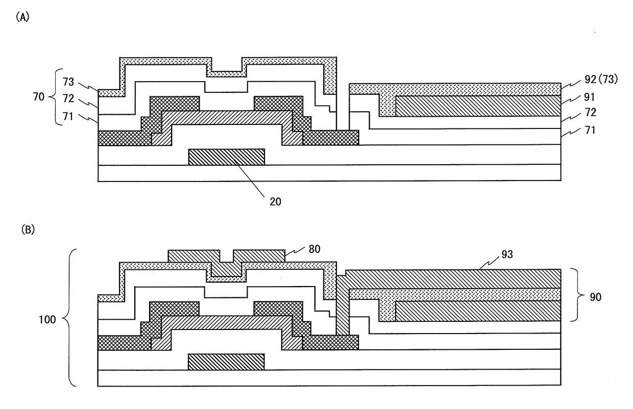
[0074]The structure of a TFT according to a first embodiment of the present invention, along with a method for manufacturing the TFT, will be described with reference to the drawings.

[0075]FIG. 1 provides a top view and a cross-sectional view illustrating the structure of the TFT 100 according to the first embodiment of the present invention; more specifically, FIG. 1(A) is the top view of the TFT 100, and FIG. 1(B) is the cross-sectional view of the TFT 100 taken along long-dash dot line A-A′ shown in FIG. 1(A). Note that in FIG. 1(A), a gate insulating film 30 and a passivation film 70 shown in FIG. 1(B) are omitted for the sake of clarity.

[0076]As shown in FIGS. 1(A) and 1(B), there is a bottom-gate electrode 20 formed on a substrate 10 such as a glass substrate. The bottom-gate electrode 20 is a film stack obtained by stacking, sequentially from the substrate 10 side, a titanium (Ti) film with a thickness of from 40 to 60 nm, an aluminum (Al) film with a thick...

second embodiment

2. Second Embodiment

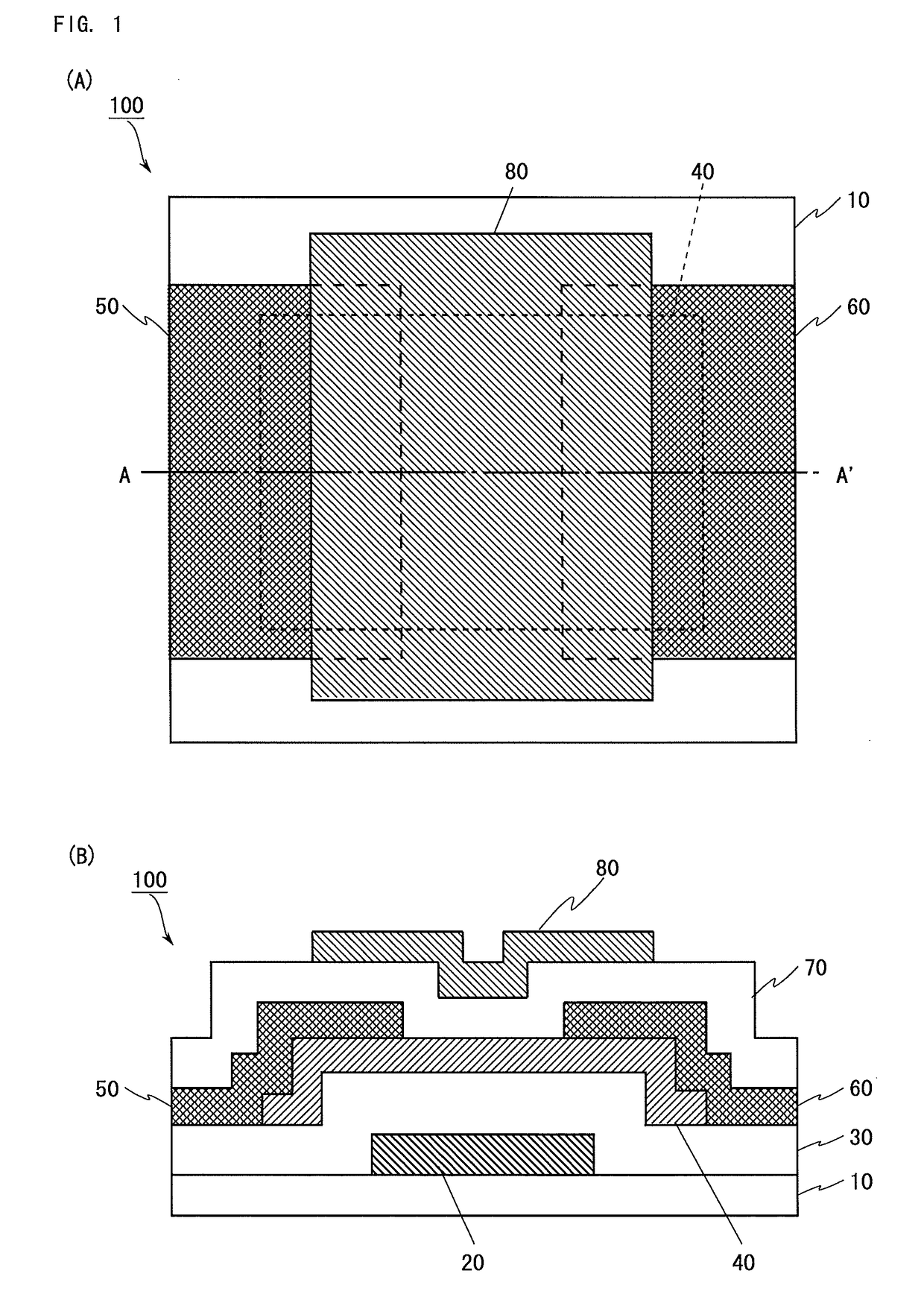
[0120]The structure of a TFT according to a second embodiment of the present invention, along with a method for manufacturing the TFT, will be described with reference to the drawings.

[0121]The basic structure of the TFT according to the present embodiment is the same as the structure of the TFT 100 shown in FIGS. 1(A) and 1(B), and therefore, features different from those of the TFT 100 according to the first embodiment will be mainly described with reference to FIGS. 1(A) and 1(B) while the same features will be described briefly.

[0122]As shown in FIGS. 1(A) and 1(B), there is a bottom-gate electrode 20 formed on a substrate 10 such as a glass substrate. On the bottom-gate electrode 20, a gate insulating film 30 is formed. Unlike in the first embodiment, the gate insulating film 30 is a film stack consisting of a total of three layers, including two silicon nitride films with different hydrogen contents and a silicon oxide film stacked on the silicon nitride fi...

third embodiment

3. Third Embodiment

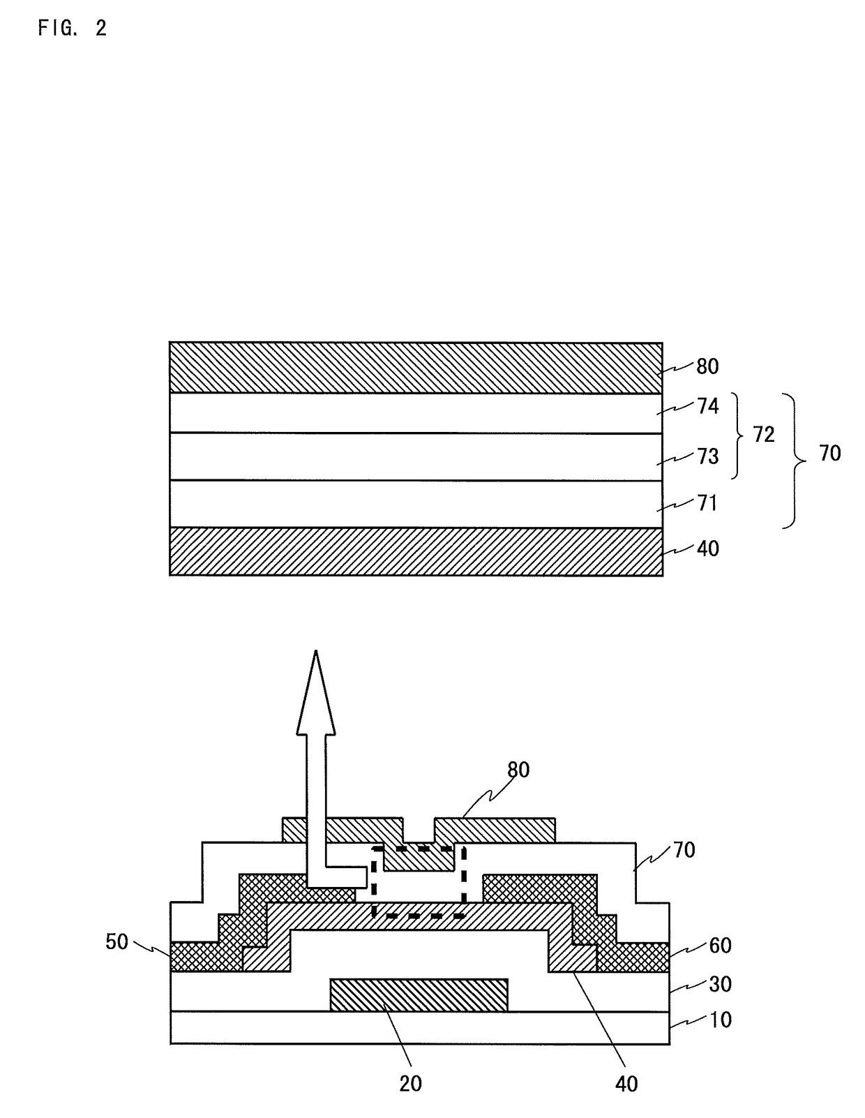
[0145]The structure of a TFT according to a third embodiment of the present invention, along with a method for manufacturing the TFT, will be described with reference to the drawings.

[0146]The basic structure of the TFT according to the present embodiment is the same as the structure of the TFT 100 shown in FIG. 1, and therefore, features different from those of the TFT 100 according to the first embodiment will be mainly described with reference to FIGS. 1(A) and 1(B) while the same features will be described briefly.

[0147]As shown in FIGS. 1(A) and 1(B), the bottom-gate electrode 20 is formed on the substrate 10 such as a glass substrate. In the TFT according to the present embodiment, unlike in the TFT 100 according to the first embodiment, the gate insulating film 30 includes a silicon nitride film 32 consisting of two layers with different hydrogen contents, as in the case of the passivation film 70. More specifically, the silicon nitride film 32 consists of ...


PUM


Abstract

Provided is a semiconductor device which has a double-gate structure with a channel layer made of an oxide semiconductor and is capable of inhibiting the occurrence of hysteresis.
A TFT having a double-gate structure with a channel layer 40 made of an oxide semiconductor uses a passivation film (70), which is a film stack obtained by stacking, sequentially from the side closest to the channel layer (40), a silicon oxide film (71), a first silicon nitride film (73), and a second silicon nitride film (74). In this case, the second silicon nitride film (74) farthest from the channel layer (40) is formed so as to have a higher hydrogen content than the first silicon nitride film (73) closer to the channel layer (40). Thus, it is rendered possible to inhibit the shifting of a threshold voltage of the TFT (100) resulting from hydrogen spreading in the channel layer (40), and at the same time, it is also rendered possible to diminish hysteresis and thereby inhibit the shifting of the threshold voltage caused by hysteresis.

Description

TECHNICAL FIELD[0001]The present invention relates to semiconductor devices and methods for manufacturing the same, particularly to a semiconductor device having a double-gate structure with a channel layer made of an oxide semiconductor and a method for manufacturing the same.BACKGROUND ART[0002]Conventionally, channel layers of thin-film transistors (TFTs) used in liquid crystal display devices, organic EL display devices, and the like are formed using silicon semiconductors such as amorphous silicon, polycrystalline silicon, or monocrystalline silicon.[0003]Recent years have seen active development of TFTs using oxide semiconductors, in place of silicon semiconductors, with a view to reducing the leakage current that flows through the TFTs in OFF state. When hydrogen and nitrogen spread in such an oxide semiconductor, these substances become sources of carrier generation, leading to a shift in TFT threshold voltage.[0004]Therefore, Patent Document 1 discloses that, to inhibit hyd...

Claims


Application Information

Patent Timeline
IPC IPC(8): H01L29/786H01L29/66H01L29/49H01L29/24H01L27/12H01L21/44H01L21/02
CPCH01L29/78606H01L27/1225H01L27/1255H01L29/7869H01L29/78648H01L21/0234H01L29/4908H01L29/66969H01L21/44H01L21/0217H01L29/24
Inventor ITO, KAZUATSUKANZAKI, YOHSUKESAITOH, TAKAO
Owner SHARP KK
Why Eureka
Try Eureka