Structure for radiofrequency applications

a radiofrequency and structure technology, applied in the direction of semiconductor devices, piezoelectric/electrostrictive/magnetostrictive devices, cell components, etc., can solve the problems of non-linear distortion of signals (harmonics), ever-increasing linkage between, and unnecessary consumption of a portion of signal energy, so as to achieve good stability and repeatability of rf performances

Active Publication Date: 2017-11-16
S O I TEC SILICON ON INSULATOR THECHNOLOGIES
View PDF4 Cites 16 Cited by
  • Summary
  • Abstract
  • Description
  • Claims
  • Application Information

AI Technical Summary

Benefits of technology

[0016]The structure for radiofrequency applications according to the disclosure, therefore, displays temperature-stable electrical properties, ensuring good stability and repeatability of the RF performances within the range of temperatures of use.

Problems solved by technology

However, the rise in the level of integration and in the performances expected of these devices results in an ever-increasing linkage between their performances and the characteristics of the substrate on which they are formed.
This results in problems of non-linear distortion of the signal (harmonics), unnecessary consumption of a portion of the energy of the signal by insertion loss and possible influences among components.
For example, antenna switches and power amplifiers manufactured on this type of substrate display very good merit factors, but are mainly used for niche applications owing to the overall cost of the solution.
Nevertheless, these substrates fail to fulfil the most stringent specifications; for example, when localized heating beyond approximately 80° C. occurs, the resistivity of these substrates declines due to generation of heat carriers in the substrate and device / substrate coupling once again becomes a major contributor to attenuation and distortion of the signal and interference among components.

Method used


Image

  • Structure for radiofrequency applications
  • Structure for radiofrequency applications
  • Structure for radiofrequency applications

Examples


first embodiment

[0065]According to the disclosure, the structure 1 for radiofrequency applications may adopt the form of a wafer with dimensions compatible with microelectronic processes, for example, of a diameter of 200 mm or 300 mm, comprising the supporting substrate 2 and the trapping layer 3. The latter may be produced according to the first or second example mentioned above, though these manufacturing examples are nevertheless not exhaustive.

second embodiment

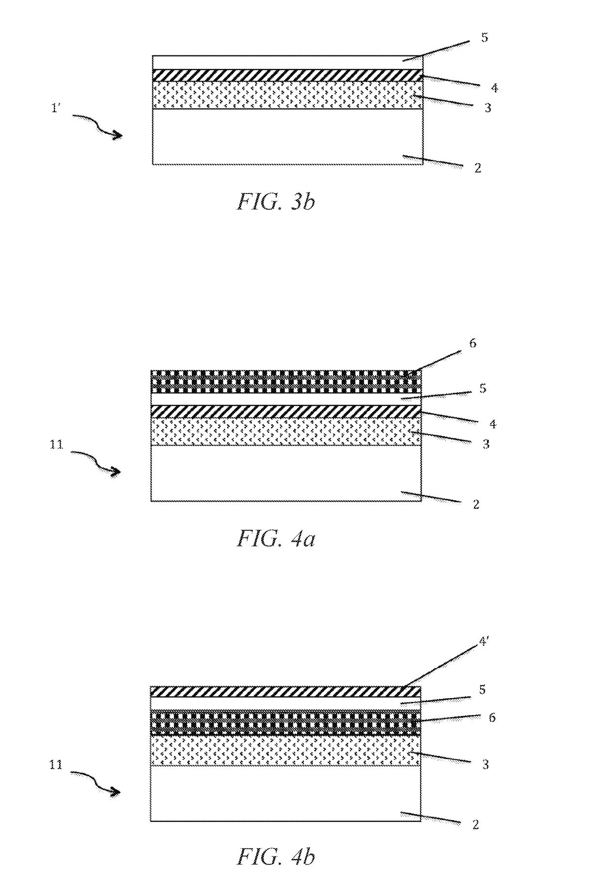
[0066]According to the disclosure illustrated in FIG. 3a, the structure for radiofrequency applications may adopt the form of a wafer and furthermore comprise an active layer 5, arranged on the trapping layer 3, in and on which it will be possible to produce RF components. The active layer 5 may advantageously consist of semiconductive materials and / or piezoelectric materials. Advantageously, without being restrictive, however, the active layer 5 comprises at least one of the materials from among silicon, silicon carbide, silicon germanium, lithium nobiate, lithium tantalate, quartz and aluminum nitride. The thickness of the active layer 5 may vary between a few nanometers (10 nm, for example) and several tens of microns (50 μm, for example) according to the components to be manufactured.

[0067]By way of example, the active layer 5 is transferred to a supporting substrate 2 comprising the trapping layer 3, using one of the methods of transferring thin layers well known to the person ...

third embodiment

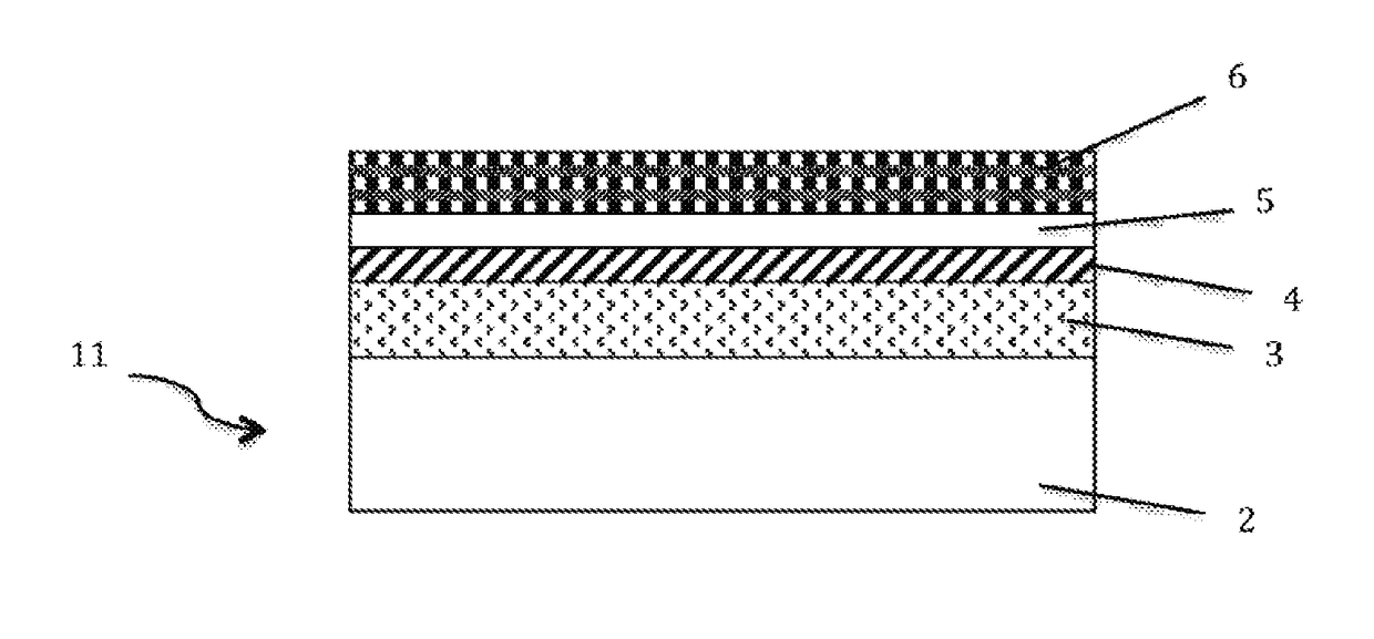
[0073] illustrated in FIG. 4a, the structure 11 for radiofrequency applications may also comprise or consist of a microelectronic device 6 on or in the active layer 5, wherein the latter is arranged on a dielectric layer 4 or directly on the trapping layer 3. The microelectronic device 6 may be a switching circuit, an adaptation or tuner circuit or even a power amplifier circuit, produced using silicon microelectronics technologies. The silicon active layer 5 typically has a thickness of between 50 nm and 180 nm, for example, 145 nm and the underlying dielectric layer 4 has a thickness of between 50 nm and 400 nm, for example, 200 nm; the trapping layer 3 is arranged between the dielectric layer 4 and the supporting substrate 2. The microelectronic device 6 produced in and on the active layer 5 comprises a plurality of active components (of the MOS, bipolar type, etc.) and a plurality of passive components (of the capacitance, inductance, resistor, resonator and filter type, etc.). ...


PUM

PropertyMeasurementUnit
temperatureaaaaaaaaaa
electrical resistivityaaaaaaaaaa
resistivityaaaaaaaaaa

Abstract

A structure for radiofrequency applications includes: a semiconducting supporting substrate, and a trapping layer arranged on the supporting substrate. The trapping layer includes a higher defect density than a predetermined defect density. The predetermined defect density is the defect density beyond which the electric resistivity of the trapping layer is no lower 10,000 ohm·cm over a temperature range extending from −20° C. to 120° C.

Description

CROSS-REFERENCE TO RELATED APPLICATIONS[0001]This application is a national phase entry under 35 U.S.C. §371 of International Patent Application PCT / FR2015 / 052494, filed Sep. 17, 2015, designating the United States of America and published as International Patent Publication WO 2016 / 087728 A1 on Jun. 9, 2016, which claims the benefit under Article 8 of the Patent Cooperation Treaty to French Patent Application Serial No. 1402801, filed Dec. 4, 2014.TECHNICAL FIELD[0002]This disclosure relates to the field of integrated radiofrequency devicesBACKGROUND[0003]Integrated devices are usually produced on substrates in the form of wafers, which mainly serve as a medium for their manufacture. However, the rise in the level of integration and in the performances expected of these devices results in an ever-increasing linkage between their performances and the characteristics of the substrate on which they are formed. This is particularly the case of radiofrequency (RF) devices processing sig...

Claims


Application Information

Patent Timeline
Patent Type & Authority Applications(United States)
IPC IPC(8): H04B1/03H01M4/66H01L21/02H01L21/28H01L21/762H01L41/047
CPCH04B1/03H01M4/663H01L21/02381H01L21/28282H01L21/02167H01L21/76297H01L41/0477H01L21/02378H01L21/02529H01L21/02532H01L21/0262H01L21/76254H01L29/40117Y02E60/10H01L21/3226H10N30/877
Inventor KONONCHUK, OLEGLANDRU, DIDIERFIGUET, CHRISTOPHE
Owner S O I TEC SILICON ON INSULATOR THECHNOLOGIES
Why Eureka
Try Eureka