Semiconductor device

Active Publication Date: 2018-01-04
MITSUBISHI ELECTRIC CORP
View PDF6 Cites 10 Cited by
  • Summary
  • Abstract
  • Description
  • Claims
  • Application Information

AI Technical Summary

Benefits of technology

[0012]According to the invention, a thinly-molded portion covering a heat dissipating portion of a lead frame and a lead frame space filled portion are integrally molded from a second mold resin, because of which adhesion between the thinly-molded portion and lead frame improves owing to the lead frame space filled portion adhering to a side surface of the lead frame. Also, as the thinly-mold

Problems solved by technology

As a power semiconductor device includes a high-heat generating element in an interior thereof, high heat dissipation is required of the mold resin.
Meanwhile, when sealing

Method used


Image

  • Semiconductor device
  • Semiconductor device
  • Semiconductor device

Examples


first embodiment

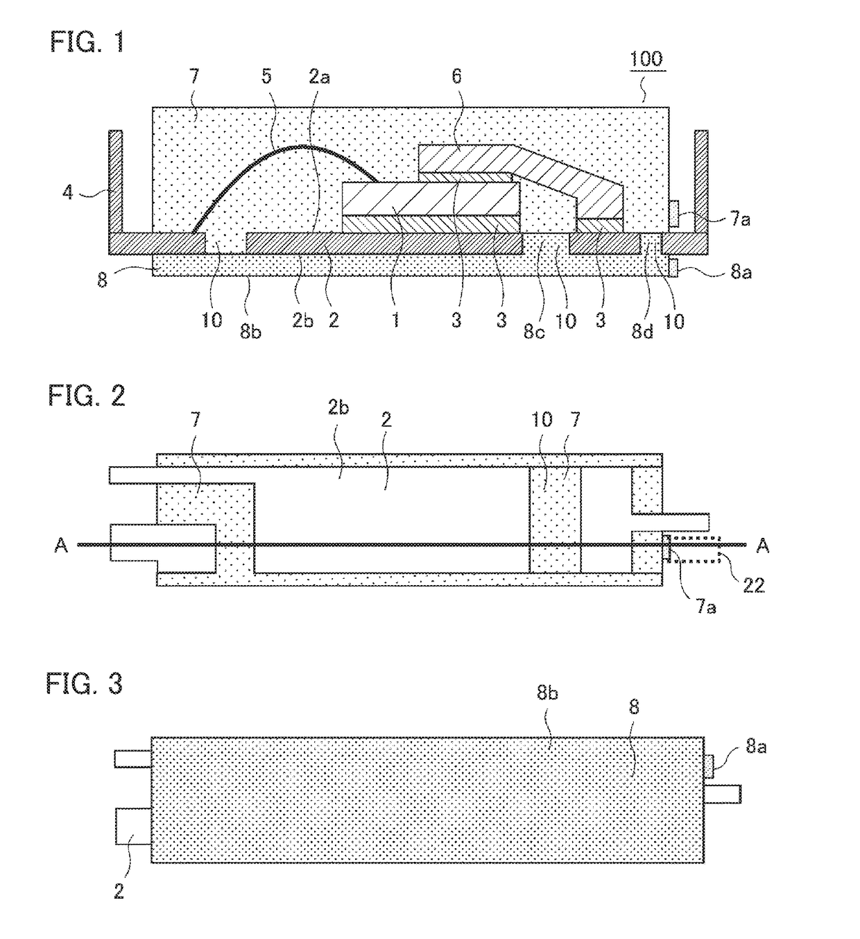
[0035]Hereafter, based on the drawings, a description will be given of a semiconductor device according to a first embodiment of the invention. FIG. 1 is a sectional view showing a configuration of a mold resin type of semiconductor device according to the first embodiment, FIG. 2 is a plan view of the semiconductor device seen from a heat dissipating surface side after a first transfer molding step, and FIG. 3 is a plan view of the semiconductor device seen from the heat dissipating surface side after a second transfer molding step. Identical or corresponding portions in the drawings are allotted the same reference signs.

[0036]As shown in FIG. 1, a semiconductor device 100 according to the first embodiment is configured to include a semiconductor element 1, a lead frame 2, an external terminal 4, a wire 5, an inner lead 6, and the like. In the example shown in FIG. 1, a mounting portion of the lead frame 2 is such that the semiconductor element 1, which is an IGBT, MOSFET, IC chip,...

second embodiment

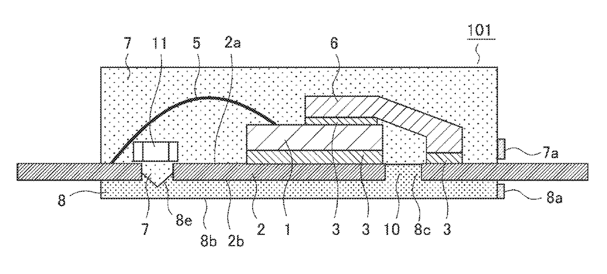
[0057]FIG. 8 is a sectional view showing a configuration of a semiconductor device according to a second embodiment of the invention. A semiconductor device 101 according to the second embodiment is a modification of the semiconductor device 100 according to the first embodiment, and as an overall configuration is the same, only differences will be described.

[0058]The semiconductor device 101 includes an electronic part (hereafter called a bridge-mounted part 11) bridge-mounted so as to straddle the die pad space 10 of the lead frame 2. A depression 8e is provided in the second mold resin 8 corresponding to directly below the bridge-mounted part 11, the mounting surface 2a of the lead frame 2 is sealed with the first mold resin 7, and the depression 8e is filled with the first mold resin 7.

[0059]Using FIG. 9, a description will be given of a manufacturing process of the semiconductor device 101 according to the second embodiment. Manufacture of the semiconductor device 101 includes ...

third embodiment

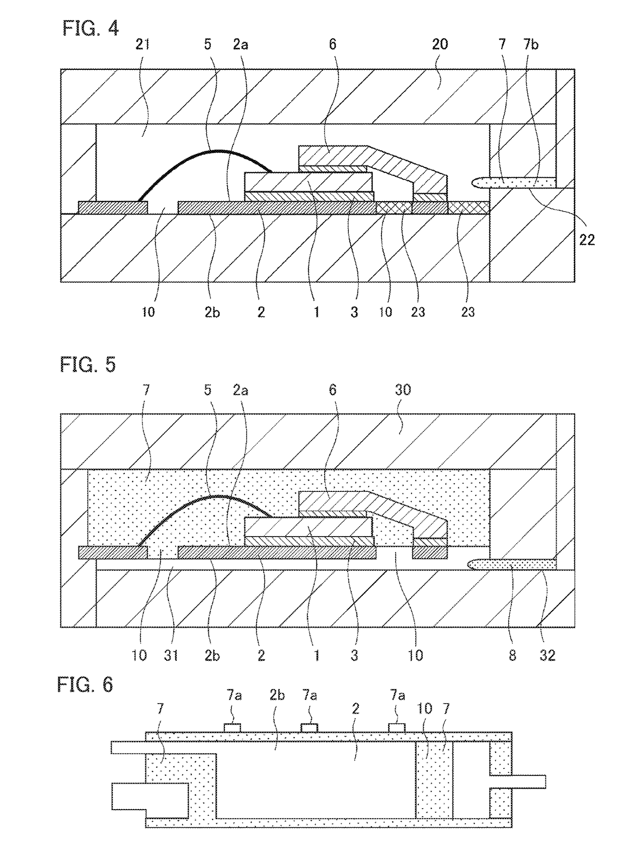
[0066]FIG. 11 is a diagram of a scanning electron micrograph showing a surface state of a lead frame of a semiconductor device according to a third embodiment of the invention. As an overall configuration of the semiconductor device according to the third embodiment is the same as in the first embodiment, a description of each component will be omitted (refer to FIG. 1). Also, as a manufacturing method of the semiconductor device according to the third embodiment is the same as in the first embodiment, a description will be omitted.

[0067]The semiconductor device according to the third embodiment uses a roughened metal plating lead frame 12 instead of the lead frame 2 used in the first embodiment. The roughened metal plating lead frame 12 is such that a surface of a lead frame 13 made of copper or a copper alloy is coated with a roughened metal plating 14 of nickel, tin, silver, gold, or the like, with a surface roughness in the region of Ra 0.06 to 0.2.

[0068]According to the third e...


PUM


Abstract

In a semiconductor device, a thinly-molded portion covering a whole of a heat dissipating surface portion of a lead frame and a die pad space filled portion are integrally molded from a second mold resin, because of which adhesion between the thinly-molded portion and lead frame improves owing to the die pad space filled portion adhering to a side surface of the lead frame. Also, as the thinly-molded portion is partially thicker owing to the die pad space filled portion, strength of the thinly-molded portion increases, and a deficiency or cracking is unlikely to occur.

Description

TECHNICAL FIELD[0001]The present invention relates to a mold resin type of semiconductor device, and in particular, relates to a semiconductor device such that the whole thereof is sealed with mold resin.BACKGROUND ART[0002]A power semiconductor device is such that a semiconductor element such as an IGBT (insulated gate bipolar transistor), MOSFET (metal-oxide-semiconductor field-effect transistor), IC chip, or LSI chip is die-bonded to an external terminal lead frame, after which an electrode of the semiconductor element and the external terminal are electrically connected by a wire or inner lead, and an input and output of signals from and to the exterior is carried out.[0003]Also, a mold resin type of semiconductor device is such that a surface on a side of the lead frame on which the semiconductor element is mounted (a mounting surface), and a heat dissipating surface on a side opposite the mounting surface, are sealed by mold resin in a molding process. As a power semiconductor...

Claims


Application Information

Patent Timeline
IPC IPC(8): H01L23/433H01L23/29H01L25/16H01L25/18H01L23/31
CPCH01L23/4334H01L23/29H01L23/31H01L25/165H01L25/18H01L2224/48091H01L2224/48247H01L2924/181H01L2224/40245H01L2224/73265H01L2224/37599H01L2224/371H01L2224/37147H01L23/3135H01L23/3142H01L23/36H01L23/49524H01L23/49548H01L23/49562H01L23/49589H01L23/49861H01L21/565H01L2224/32245H01L2924/19105H01L2224/73221H01L2924/00012H01L2924/00014H01L2924/00
Inventor KAJIHARA, TAKANOBUOMAE, KATSUHIKOFUSHIE, SHUNSUKEMUKUDA, MUNEAKINAKASHIMA, DAISUKEMOTOOKA, MASAHIROMIYANISHI, HIROYUKINAKAMATSU, YUKISUZUKI, JUNYA
Owner MITSUBISHI ELECTRIC CORP
Why Eureka
Try Eureka