
Multilayer structure, method for producing same, packaging material and product including same, and protective sheet for electronic device

a multi-layer structure and packaging material technology, applied in the direction of pharmaceutical packaging, containers preventing decay, synthetic resin layered products, etc., can solve the problems of poor packaging appearance, low light transmittance, and poor barrier performance, and achieve good gas barrier properties, good water vapor barrier properties, and good retort resistance

Active Publication Date: 2018-01-18
KURARAY CO LTD
View PDF1 Cites 7 Cited by
  • Summary
  • Abstract
  • Description
  • Claims
  • Application Information

AI Technical Summary

Benefits of technology

The present invention is a patent that describes a new multilayer structure that has good gas and water vapor barrier properties, as well as high retort resistance and transparency. The invention can be used as a packaging material for products and a protective sheet for electronic devices. It can maintain its barrier properties even after retorting and a damp heat test. Overall, the invention provides a novel solution for creating high-quality packaging and protective materials for electronic devices.

Problems solved by technology

However, in some cases where the present inventors used the multilayer structure of Patent Literature 1 as a packaging material, the appearance of the packaged substance was poor due to insufficient transparency of the multilayer structure.
In addition, in some cases where the multilayer structure was used as a packaging material for a retort food, the barrier performance deteriorated as a result of retorting.
Furthermore, in some cases where the present inventors used the multilayer structure of Patent Literature 1 in an electronic device, the light transmittance was low due to insufficient transparency of the multilayer structure.

Method used

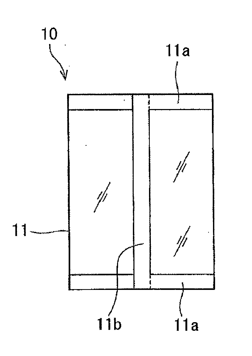
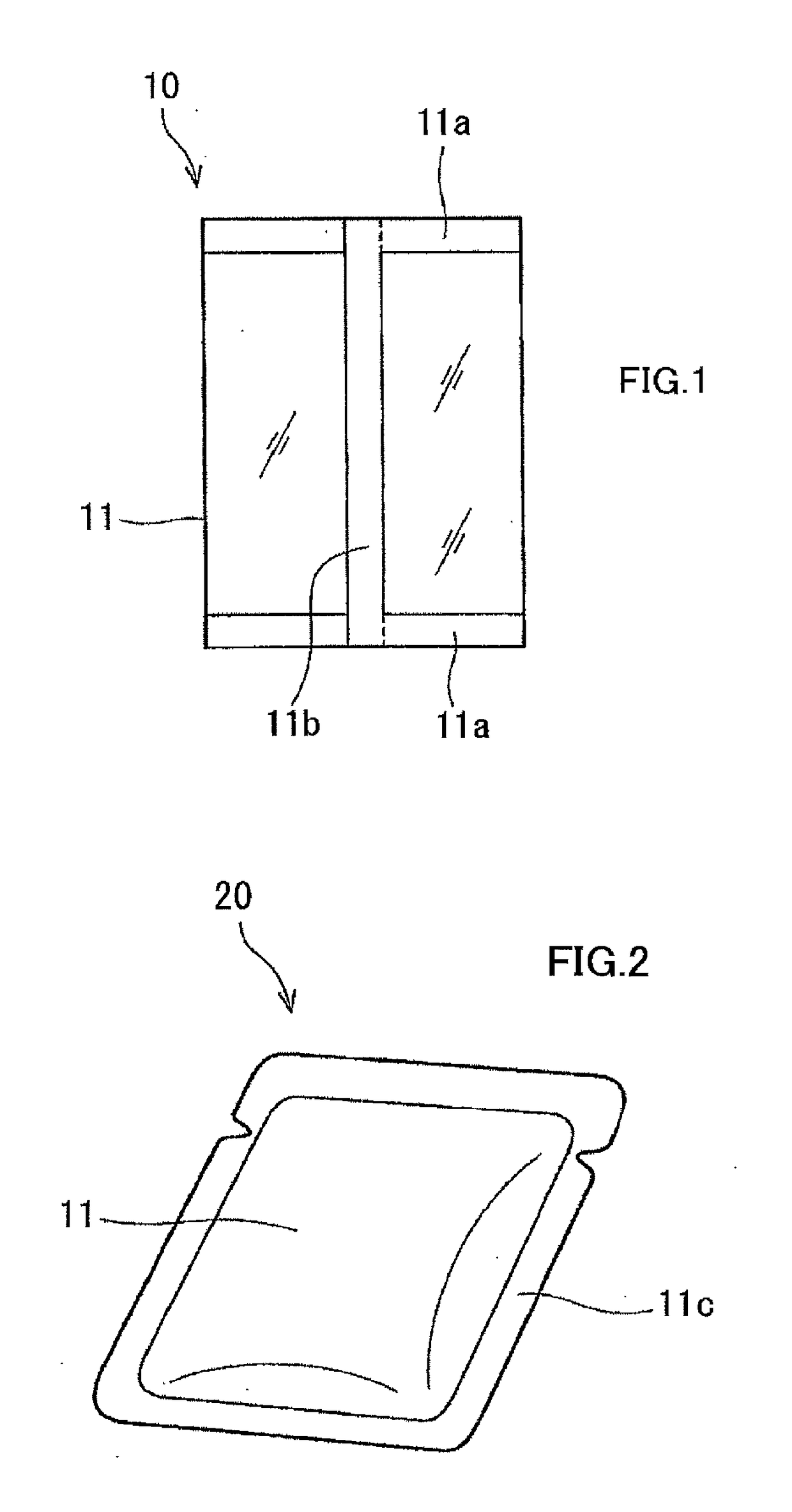
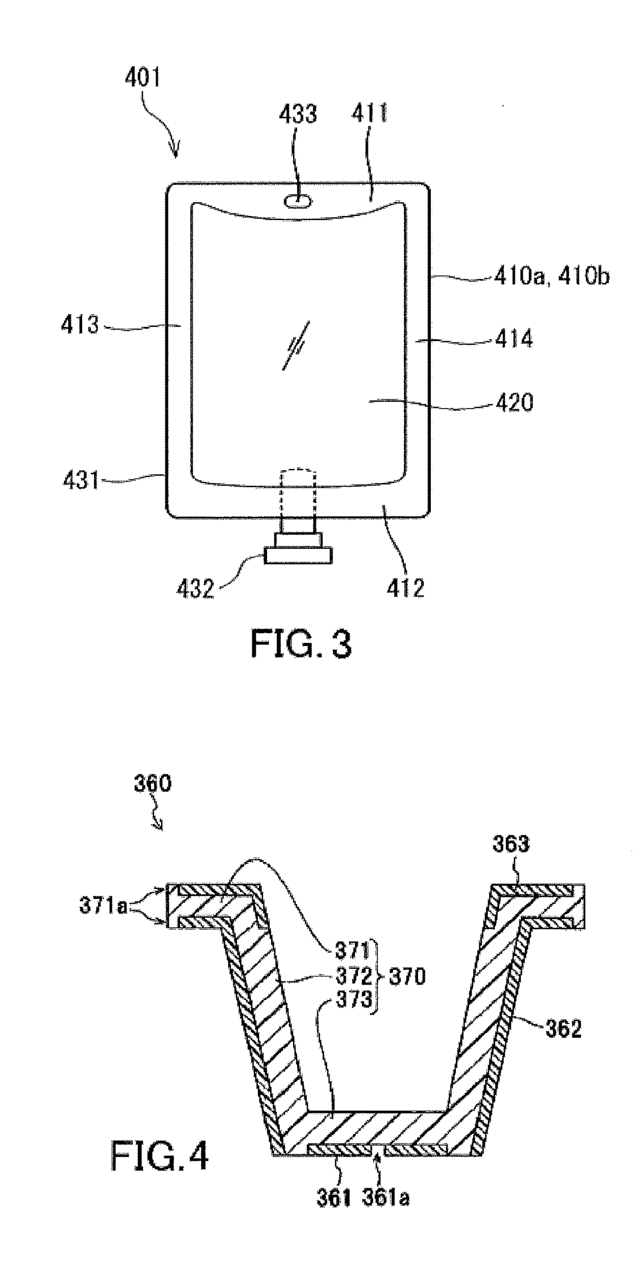

Image

  • Multilayer structure, method for producing same, packaging material and product including same, and protective sheet for electronic device
  • Multilayer structure, method for producing same, packaging material and product including same, and protective sheet for electronic device
  • Multilayer structure, method for producing same, packaging material and product including same, and protective sheet for electronic device

Examples


example 1

Example 1-1

[0333]First, a PET 12 (which may hereinafter be abbreviated as “X-1”) was prepared as the base (X). The coating liquid (S-1) was applied onto the base using a bar coater in such a manner that the dry thickness would be 0.3 μm. The film of the applied liquid was dried at 110° C. for 5 minutes to form a precursor of a layer (Y-1-1) on the base. In this way, a structure having a configuration of “base (X-1) / layer (Y-1-1) precursor” was obtained. Subsequently, the structure was heat-treated at 160° C. for 1 minute and then at 220° C. for 1 minute to form the layer (Y-1-1). In this way, a multilayer structure (1-1-1) having a configuration of “base (X-1) / layer (Y-1-1)” was obtained.

[0334]As a result of measurement of the infrared absorption spectrum of the multilayer structure (1-1-1), the maximum absorption wavenumber in the region from 800 to 1,400 cm−1 was determined to be 1,108 cm−1, and the width at half maximum of the maximum absorption band was determined to be 37 cm−1....

example 1-2

[0344]A vacuum insulator was fabricated using the multilayer structure (1-1-2) as obtained in Example 1-1. Specifically, the multilayer structure (1-1-2) was first cut into two pieces of a given shape. The two pieces of the multilayer structure (1-1-2) were then stacked together in such a manner that the CPP layers were located interiorly, and the resulting rectangular stack was heat-sealed at its three sides to form a bag. Next, a heat-insulating core material was put into the bag through the opening of the bag, and the bag was hermetically closed using a vacuum packaging machine (VAC-STAR 2500, manufactured by Frimark GmbH) so that the internal pressure was 10 Pa at a temperature of 20° C. In this way, a vacuum insulator was successfully fabricated without any problem. The heat-insulating core material used was a fine silica powder dried at 120° C. for 4 hours.

example 1-3

[0345]A solar cell module was fabricated using the multilayer structure (1-1-1) as obtained in Example 1-1. Specifically, first, an amorphous silicon solar cell placed on a 10-cm-square tempered glass plate was sandwiched between ethylene-vinyl acetate copolymer films with a thickness of 450 μm. The multilayer structure (1-1-1) was then bonded onto one of the films in such a manner that the PET layer of the multilayer structure (1-1-1) faced outwardly. In this way, a solar cell module was fabricated. The bonding was accomplished by vacuum drawing at 150° C. for 3 minutes, followed by compression bonding for 9 minutes. The solar cell module thus fabricated operated well and continued to show good electrical output characteristics over a long period of time.


PUM

PropertyMeasurementUnit
particle diameteraaaaaaaaaa
temperatureaaaaaaaaaa
particle diameteraaaaaaaaaa

Abstract

The present invention relates to a multilayer structure including a base (X) and a layer (Y) stacked on the base (X). The layer (Y) contains a reaction product (D) of an aluminum-containing compound (A) and a phosphorus compound (B), and the reaction product (D) has an average particle diameter of 5 to 70 nm.

Description

TECHNICAL FIELD[0001]The present invention relates to a multilayer structure, a method for producing the multilayer structure, a packaging material and product including the multilayer structure, and a protective sheet for electronic devices.BACKGROUND ART[0002]Multilayer structures in which a gas barrier layer containing aluminum or aluminum oxide as a component is formed on a plastic film have been conventionally well-known. Such multilayer structures are used as packaging materials for protecting articles (such as foods) which are susceptible to quality change induced by oxygen. In many cases, such a gas barrier layer is formed on a plastic film by a dry process such as physical vapor deposition (PVD) or chemical vapor deposition (CVD). Such a multilayer structure is used also as a component of a protective sheet for an electronic device to protect the characteristics of the electronic device when the electronic device is required to have gas barrier properties and water vapor ba...

Claims


Application Information

Patent Timeline
Patent Type & Authority Applications(United States)
IPC IPC(8): B32B37/15B65D75/40B65D65/40A61J1/10H01L31/049B32B29/00B32B27/06A61J1/14H01L51/52
CPCB32B37/15B32B27/06B32B29/002B65D65/40A61J1/10A61J1/1468B65D75/40H01L31/049H01L51/5253B32B2439/46B32B2571/00H01L31/048B32B7/12B32B27/08B32B27/10B32B27/32B32B27/34B32B27/36B32B2250/03B32B2250/24B32B2255/10B32B2255/12B32B2255/26B32B2255/28B32B2307/306B32B2307/412B32B2307/7244B32B2307/7246H01L31/0481Y02E10/50H10K59/873B32B9/00B32B9/045B32B9/06B32B37/24B32B38/0036B32B38/164B65D81/24B32B2439/00H10K50/844
Inventor INUBUSHI, YASUTAKASASAKI, RYOICHIOTA, MASAHIKO
Owner KURARAY CO LTD
Learn More